


-
With the development of technology, more and more electronic devices are highly in demand for space and other radiation environments. However, the radiation effect to devices caused by energetic particles has become the main reason for the failure/damage of the on-orbit spacecrafts equipped with advance technology and modern electronic devices[1]. The single-event effect(SEE) is one of the major concerns in reliability issues because it can be induced by the incidence of a single energetic particle[2]. During the last decades, the development of the microelectronics industry has always followed Moore’s law, and the feature size of the electronics devices has been reached a scaling limit point[3]. The three dimension(3D) fin field-effect transistor(FinFET) structure has replaced planar structure and become the feature size of the semiconductor devices below 22 nm[4].
The structures of planar FET and FinFET are shown in Fig. 1. The FinFET static random access memory(SRAM) has great application prospects in the aerospace fields due to its excellent electrostatic control[5]. Previous researches have demonstrated that the FinFET technology has significant advantages over planar technology in single-event response resistance, especially for low linear energy transfer(LET) particles[6-7].
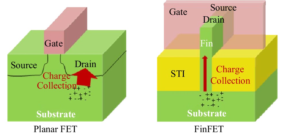
Figure 1. (color online)Sketches of the planar FET and FinFET[8].
However, advanced technologies bring new responses to the SEE. On the one hand, due to the elevated source-drain structure and low fin-to-fin distance, the inter-junction proximity is close for the FinFET device. This facilitates charge collection by multiple junctions in a single radiation strike, which may lead to a higher probability of multiple-bit upset(MBU). In memory circuits such as SRAM, the analysis of the impact of MBU is quite crucial[9-10] for various mitigation technique choices such as the degree of column interleaving and selection of error correction codes(ECC). As SRAM density increases and dimension reduces, MBU becomes a critical issue for SRAM applications in space electronic devices. On the other hand, due to the shape of the transistor, previous studies have shown that the single-event response of bulk FinFET devices is related to the incident angle of the particles[11-12]. In this paper, the single-event upset(SEU) of the 14-nm FinFET SRAM irradiated by heavy ions with different LETs is presented. The MBU contribution is also analyzed. Additionally, the influence of the anisotropic structure of FinFET is considered when the incident angle is inclined.
-
The test devices were fabricated using a commercial 14-nm bulk FinFET complementary metal-oxide-semiconductor(CMOS) technology. The capacity of the SRAM array was 128 Mbits. The device’s normal core logic supply voltage was 0.8 V, and the IO voltage was 1.8 V. The clock frequency was adjustable with a 5 MHz minimum value to meet system timing requirements. The area of one memory cell was approximately 0.067 μm2. The information about the device is listed in Table 1.
Table 1. Information of the device.
Paraments Value Technology 14 nm, FinFET CMOS, Flip-Chip Packaged Die area 6.17 mm × 17.87 mm Core voltage/IO voltage 0.8 V/1.8 V Array dimension 128 Mbits Cell area 0.18 μm × 0.37 μm Fin height/Fin width 45 nm/15 nm Fin pitch/Contacted
gate pitch46 nm/85 nm A homemade test system was consisted of a robust mainboard and a replaceable DUT board. The main board receives the request command from the host. Data operations such as write/read/compare/correct were performed to run the DUT. The motherboard use to read the current value of DUT in real time along-with a record of the detected error details. Then, it was being uploaded to the host through Ethernet as the communication port. The mainboard and DUT board can transmit signals and powers by 180 differential pairs- channels through four Samtec’s high-speed connectors. There was no other device placed nearby the irradiation region. The current of the DUT power components was continuously monitored and displayed in real-time. Slight voltage variations were probed and multiplied by a precision resistor and current sense amplifier, which were afterward converted to a digital form that can be handled by an FPGA rely on a 12-bit ADC. The DUT currents were monitored at one-second intervals.
-
The tests of heavy-ion irradiation were performed at the Heavy Ion Research Facility in Lanzhou(HIRFL) and HI-13 Tandem Accelerator in Beijing. Experiments were carried out with different broad beam ion species including 12C, 19F, 78Kr and 86Kr. The heavy ions’ LET at the sensitive volume(SV) surface is range from 2.4 to 40.3 MeV/(mg/cm2). The detailed experimental parameters used in this experiment are provided in Table 2. The heavy ions’ LET values and the projected ranges in silicon were calculated by the Stopping and Range of Ions in Matter (SRIM) software[13]. All tests were conducted at a normal voltage of 0.8 V and room temperature.
Table 2. Parameters of Heavy Ions Used in the Experiment.
Terminal Ion
speciesEnergy*/
MeVLET */
[MeV/(mg·cm–2)]Penetration depth/
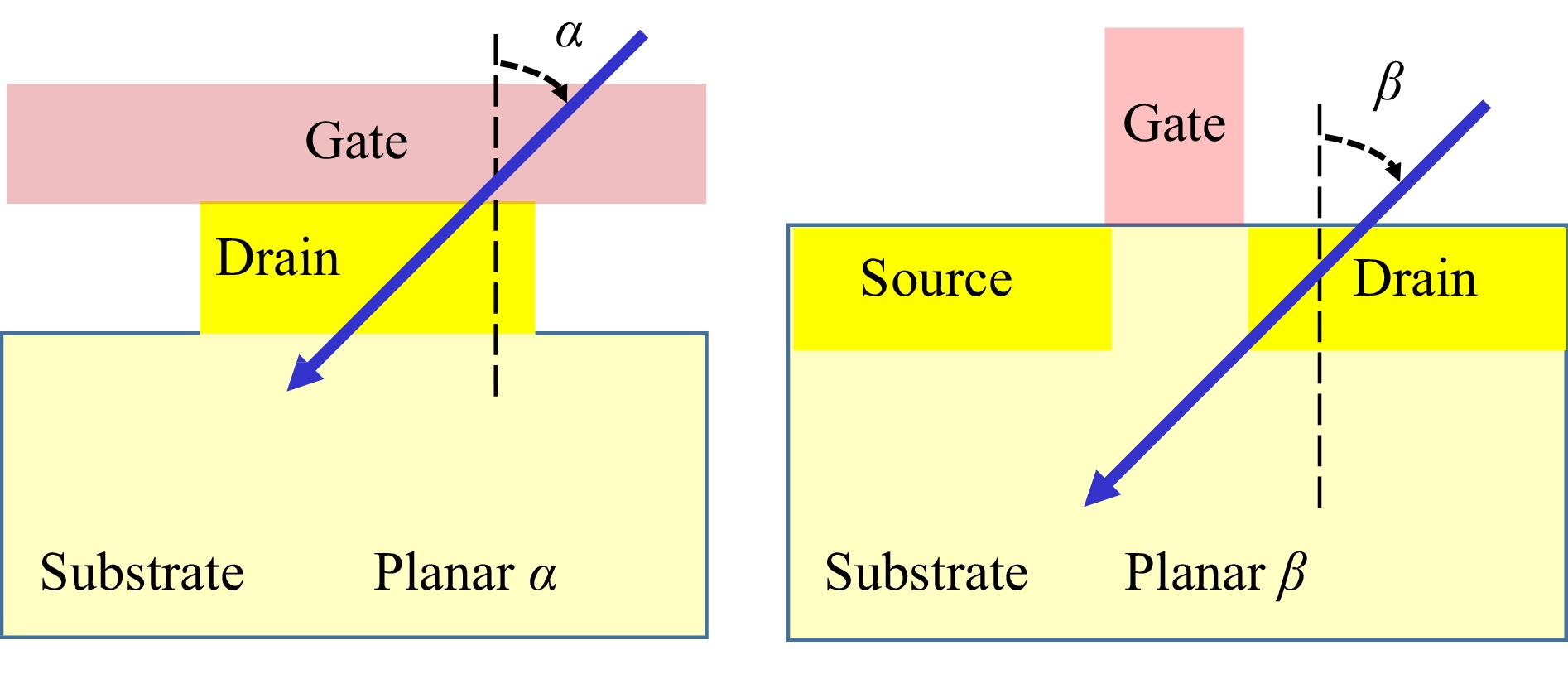
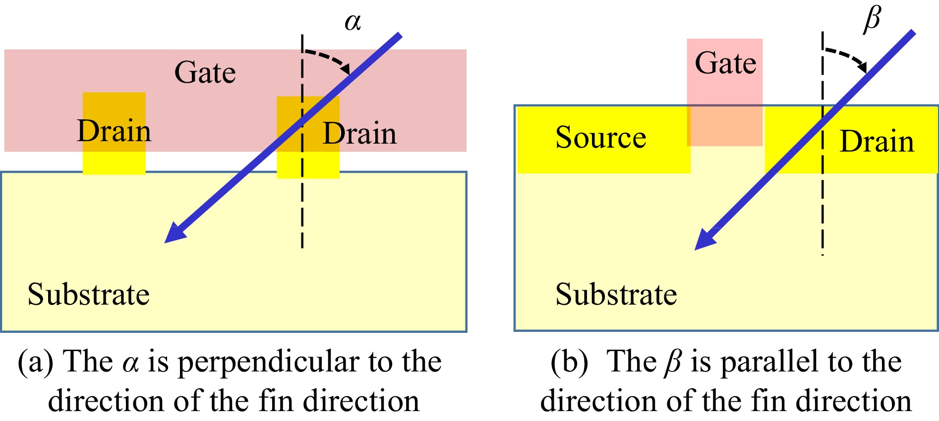
range in Si/μmHI-13 12C 52 2.6 67 19F 47 6.3 28 HIRFL 78Kr 3578 12.7 775 2210 17.4 373 86Kr 1371 24.7 185 904 30.6 112 294 40.3 38 *At the surface of SV. Additionally, the 78Kr ions with initial energy 3 751 MeV were carried out at different angles incidence relative to two axes: 30°, 45° and 60°, as shown in Fig. 2(d) and (e). Fig. 2 shows the fin structure and the incident angle relative to the fin structure. The BC axis is parallel to fin direction, and the angle of the DUT around the BC axis is marked as α angle. The AB axis is perpendicular to fin direction, and the angle of the DUT around the AB axis is marked as β angle.
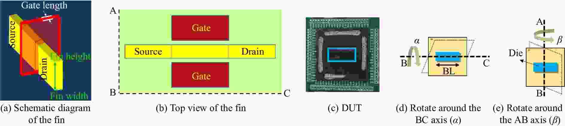
Figure 2. (color online)The fin structure and the incident angle relative to the fin structure.
-
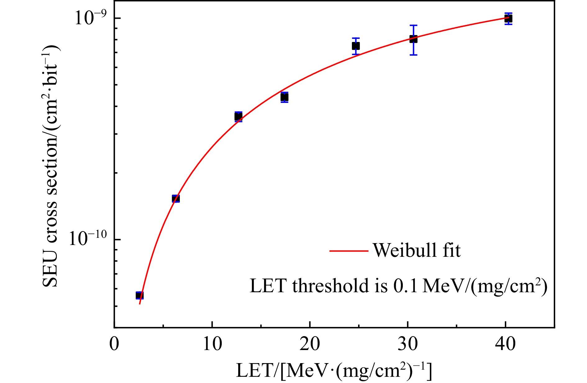
The SEU cross-section (σ) in the unit of cm2/bit for a bulk FinFET SRAM can be calculated by the following equation:
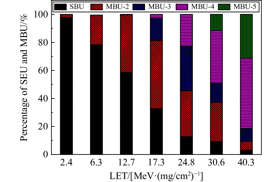
$$ \sigma =\frac{N}{{N}_{\rm b}}\times F\times \mathrm{cos}\theta, $$ where N represents the total number of errors, Nb is the number of bits in the device, θ is the angle of incidence, and F is the ion fluence in ions/cm2. The SEU cross-section as a function of LET for 14-nm flip-chip packaged bulk FinFET SRAM is shown in Fig. 3. Error bars in all the plots of this paper represent standard errors. The figure shows that the SEU cross-section increases with LET value even if the LET value is larger than 24.7 MeV/(mg/cm2). The LET threshold is 0.1 MeV/(mg/cm2) obtained by fitting the SEU cross-section using the Weibull function. The reason of section unsaturation is related to MBU. As shown in Fig. 4, the contribution of the MBU is obvious increasing with LET. In this figure, SBU presents single-bit upset. MBU-2 presents double-bit upsets. MBU-3 presents triple-bit upsets. MBU-4 presents quadruple-bit upsets. MBU-5 presents quintuple-bit upsets. With the increase of LET, the proportion of the SBU decreases, while the proportion of the maximum number of upsets increases. The proportion of the MBU between them always increases first and then decreases. As the LET equals to 2.4 MeV/ (mg/cm2), most patterns of upset are the SBU. However, the contribution of the MBU is greater than 95%, which becomes the main SEU component when the LET is equal to 40.3 MeV/(mg/cm2).

Figure 3. (color online)The SEU cross-section of 14-nm FinFET SRAM versus the LET of incident heavy ions.
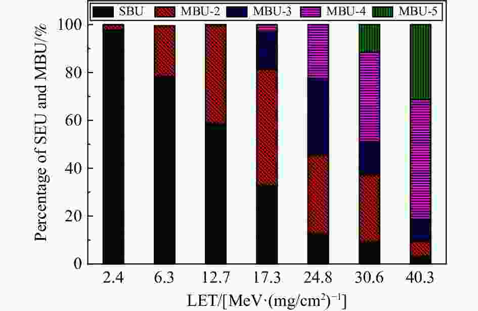
Figure 4. (color online)The percentage of different upset patterns varies with the LET of incident heavy ions.
In silicon-based SRAM devices, the dominant reasons for the MBU are charge sharing, bipolar amplification, secondary ions, and peripheral circuits[14]. For bulk FinFET SRAM devices, charge sharing is the key point. Firstly, the diameter of charge deposition from a single heavy ion covers multiple sensitive units. Secondly, the deposited charge of the ions on the substrate, including the sub-fin, would influence the MBU through diffusion. And the charge collected from the substrate is limited due to the narrow connection between the drain and the substrate of the bulk FinFET device. The charge sharing is enhanced due to the influence region of the ion-track structure increasing with the LET. The radial distribution of charges generated around an ion-track is an important factor for MBU induced by high-LET ions, especially in nanoscale devices like the ones used in the current study. For the FinFET technology, the ion-track radius needs to be considered because it is larger than the device dimensions like gate length and fin width.
-
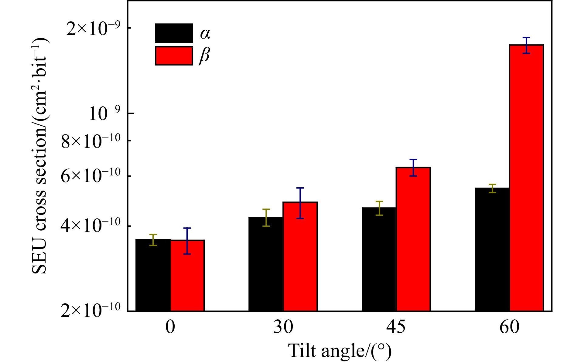
As shown in Fig. 2(d) and (e), with respect to the two different directions of the fin structure, three incident angles of 78Kr ions with the same initial energy (3 751 MeV) were used to investigate the impact of incident angles on SEU. The SEU cross-section versus incident angle is shown in Fig. 5. In this figure, the SEU cross-section increases with the angle of incidence. Perpendicular to the fin direction (α), from 0° to 60°, the SEU cross-section increased by only 1.5 times. While parallel to the fin direction (β), it is increased by 4.9 times. The phenomenon of increasing the SEU cross-section with the β angle is similar to that in a planar device. As shown in Fig. 6 and Fig. 7, when the incident angle is β, the charge deposition path in FinFET is similar to that in a planar device.
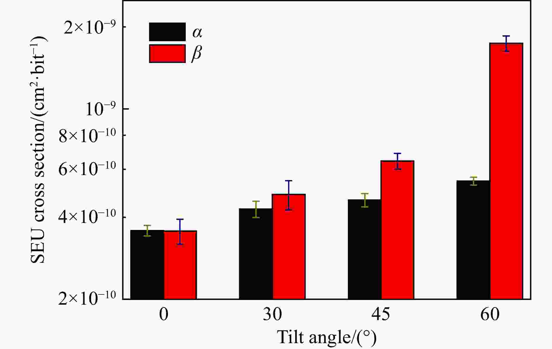
Figure 5. (color online)The SEU cross-section versus the incident angle of heavy ions.
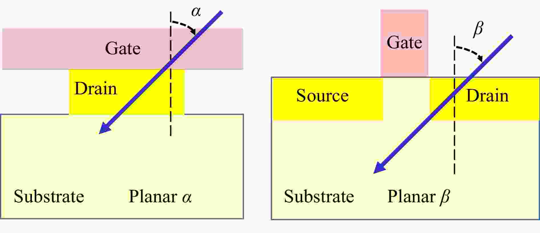
Figure 6. (color online)The cross-section view of traditional planar transistor.
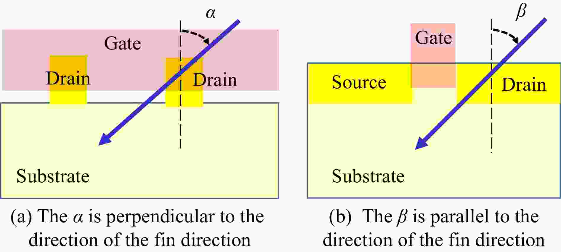
Figure 7. (color online)The cross-section view of FinFET.
The uniqueness of the geometry structure of FinFET determines the characteristic of its angular effect. On the one hand, when the ions are incident at α angle as shown in Fig. 7(a), for most of the events, edge effect (the track length of ion in the SV is not arc-cosine law) will occur because the SV of the FinFET device is narrow and high. This is different from the traditional planar device as shown in Fig. 6. It will drop the track length of the ions in the SV. The decrease of the ion track length in the SV may lead to the decrease of SEU cross-section due to the decrease/drop of the collected charge. However, when the ions are incident at β angle, the track length of incident ions in the SV follows a similar trend of like planar bulk technologies as shown in Fig. 6 and Fig. 7(b). It will raise the track length of the ions in the SV for most of the events, which leads to an increase of the collected charge.
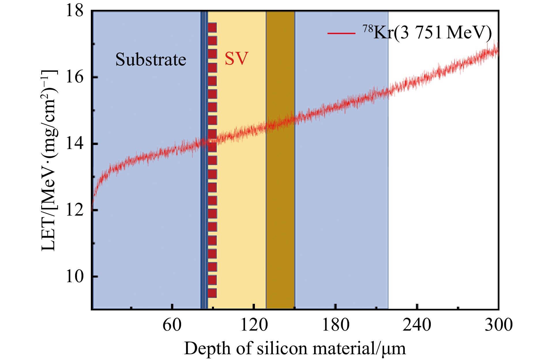
On the other hand, as the device is a flip chip package device, all the ions before reaching the SV must pass through the substrate- acting as a natural energy degrader. As shown in Fig. 8, the curve represents the LET of 78Kr ion with an initial energy of 3 751 MeV as a function of incident depth in silicon. With the increase of the incident angle, the traverse length of ions through the substrate increases, resulting in the increase of LET value for the ions reaching the SV surface. In summary, the inconsistent change of charge deposition path of ions in SV caused by the characteristics of SV shape is the reason for the SEU cross-section changed differently with α angle and β angle.
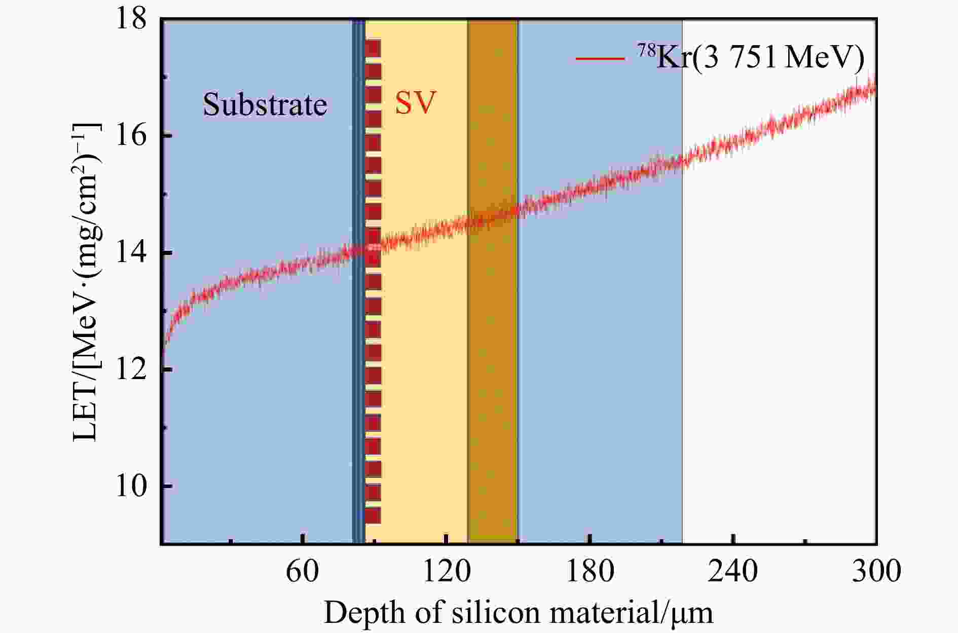
Figure 8. (color online)LET dependence of 78Kr ion (initial energy 3 751 MeV) with incident depth in silicon.
-
This work investigates the impacts of LET on the SEU cross-section and MBU contribution induced by heavy ions for 14-nm bulk FinFET SRAM. Based on the anisotropic structure of the FinFET, the impact of angular effects on SEU cross-section induced by heavy ions are also investigated. The results show that MBU is a critical issue for high-LET heavy ion irradiation, due to increasing SRAM device density and scaled dimensions. The SEU cross-section of 14-nm bulk FinFET SRAMs exhibits strong dependence on geometry and orientation. When the incident angle is parallel or is perpendicular to the direction of the fin direction, the variation trend of the SEU cross-section is inconsistent, which is different from the planar device. These results are useful to design of radiation-hardened CMOS integrated circuits(ICs) in the FinFET technology, suggesting the requirement of future investigations to be carried out on the impacts of track dimension and charge sharing in FinFET SRAM.
-
摘要: 通过重离子实验研究了14-nm FinFET工艺静态随机存取存储器(SRAM)的单粒子翻转(SEU)特性。通过使用Weibull函数拟合SEU截面获得该器件的线性能量转移(LET)阈值:0.1 MeV/(mg/cm2)。对多位翻转(MBU)贡献的统计结果表明,当LET等于40.3 MeV/(mg/cm2)时,MBU的占比超过95%。此外,FinFET SRAM的SEU截面呈现出与Fin相关的入射角度的各向异性。该研究对基于FinFET工艺的抗辐射CMOS集成电路(IC)的设计具有一定的指导作用。
-
关键词:
- FinFET SRAM /
- heavy ion /
- single-event upset(SEU) /
- angle effect
Abstract: The characteristic of single-event upset(SEU) in a 14-nm bulk fin field-effect transistor (FinFET) static random access memory(SRAM) is investigated by heavy-ion experiments. The linear energy transfer(LET) threshold 0.1 MeV/(mg/cm2) is obtained by fitting the SEU cross-section using the Weibull function. The contribution of multiple-bit upset(MBU) is investigated. The results show that when the LET is equal to 40.3 MeV/(mg/cm2), greater than 95% of SEU comes from the MBU. Additionally, the SEU cross-section of the FinFET SRAM presents anisotropies for incident angles associated with the fin direction. This research has a certain kind of guiding role in designing of radiation-hardened complementary metal-oxide semiconductor(CMOS) integrated circuits(ICs) based on FinFET technology.-
Key words:
- FinFET SRAM /
- heavy ion /
- single-event upset(SEU) /
- angle effect
-
Figure 2. (color online)The fin structure and the incident angle relative to the fin structure.
Figure 3. (color online)The SEU cross-section of 14-nm FinFET SRAM versus the LET of incident heavy ions.
Figure 4. (color online)The percentage of different upset patterns varies with the LET of incident heavy ions.
Figure 5. (color online)The SEU cross-section versus the incident angle of heavy ions.
Figure 8. (color online)LET dependence of 78Kr ion (initial energy 3 751 MeV) with incident depth in silicon.
Table 1. Information of the device.
Paraments Value Technology 14 nm, FinFET CMOS, Flip-Chip Packaged Die area 6.17 mm × 17.87 mm Core voltage/IO voltage 0.8 V/1.8 V Array dimension 128 Mbits Cell area 0.18 μm × 0.37 μm Fin height/Fin width 45 nm/15 nm Fin pitch/Contacted
gate pitch46 nm/85 nm  下载: 导出CSV
Table 2. Parameters of Heavy Ions Used in the Experiment.
Terminal Ion
speciesEnergy*/
MeVLET */
[MeV/(mg·cm–2)]Penetration depth/
range in Si/μmHI-13 12C 52 2.6 67 19F 47 6.3 28 HIRFL 78Kr 3578 12.7 775 2210 17.4 373 86Kr 1371 24.7 185 904 30.6 112 294 40.3 38 *At the surface of SV.
下载: 导出CSV
-
[1] ECOFFET R. On-orbit anomalies: Investigations and root cause determination[C]//IEEE NSREC 2011 Short Course Notes, Section IV. USA: Institute of Electrical and Electronics Engineers Inc, 2011: 1198. [2] BESSOT D, VELAZCO R, Design of SEU-hardened CMOS Memory Cells: the HIT cell[C]//RADECS 93. Second European Conference on Radiation and its Effects on Components and Systems (Cat. No. 93TH0616-3). USA: Institute of Electrical and Electronics Engineers, Inc, 1993: 563. [3] WALDROP M M. Nature News, 2016, 530(7589): 144. doi: 10.1038/530144a [4] COLINGE J P. 3D Transistors[C]//2013 International Symposium on VLSI Technology, Systems and Application (VLSI-TSA). USA: Institute of Electrical and Electronics Engineers, Inc, 2013: 2. [5] BANSAL A, MUKHOPADHYAY S, ROY K. IEEE Transactions on Electron Devices, 2007, 54(6): 1409. doi: 10.1109/TED.2007.895879 [6] SEIFERT N, JAHINUZZAMAN S, VELAMALA J, et al. IEEE Transactions on Nuclear Science, 2015, 62(6): 2570. doi: 10.1109/TNS.2015.2495130 [7] NSENGIYUMVA P, BALL D R, KAUPPILA J S, et al. IEEE Transactions on Nuclear Science, 2016, 63(1): 266. doi: 10.1109/TNS.2015.2508981 [8] FANG Y P, OATES A S. IEEE Transactions on Device and Materials Reliability, 2011, 11(4): 551. doi: 10.1109/TDMR.2011.2168959 [9] WU W, SEIFERT N. MBU-Calc: A Compact Model for Multi-bit Upset (MBU) SER Estimation[C]//2015 IEEE International Reliability Physics Symposium. USA: Institute of Electrical and Electronics Engineers, Inc, 2015: SE. 2.1-SE. 2.6. [10] QUINN H, GRAHAM P, Krone J, et al. IEEE Transactions on Nuclear Science, 2005, 52(6): 2455. doi: 10.1109/TNS.2005.860742 [11] ZhANG H, JIANG H, ASSIS T R, et al. IEEE Transactions on Nuclear Science, 2017, 64(1): 491. doi: 10.1109/TNS.2016.2637876 [12] NSENGIYUMVA P, MASSENGILL L W, KAUPPILA J S, et al. IEEE Transactions on Nuclear Science, 2018, 65(1): 223. doi: 10.1109/TNS.2017.2775234 [13] SRIM [EB/OL][2021-01-20]. http://www.srim.org. [14] HUBERT G, CAVOLI P L, FEDEICO C, et al. IEEE Transactions on Nuclear Science, 2015, 62(6): 2837. doi: 10.1109/TNS.2015.2496238 -

 点击查看大图

计量
- 文章访问数: 761
- HTML全文浏览量: 339
- PDF下载量: 66
- 被引次数: 0

 甘公网安备 62010202000723号