


-
Broadband response has attracted general interests in a variety of optical applications including photodetectors[1-3], photocatalysis[4-6], solar energy[7-10], infrared imaging[11-13]. For example, it has been reported that the broadband response (300~750 nm) of SnS2 flakes is significantly promoted after an oxygen plasma bombardment. Sub-bandgaps are artificially induced, as a result, the detectivity and external quantum efficiency are improved by one order of magnitude[2]. Moreover, for many photocatalysis applications, for example, CO2 reduction, broad spectral response is becoming an essential need. By tailoring the defect levels and the dopant energy levels, photo-absorption is extended from UV to visible and even to IR light range, thereby achieving broad spectral response to promote carbon dioxide photoreduction and to improve the photocatalytic efficiency[4]. Among various nanostructures that can lead to broad spectral response, nanocones have a great potential because of their linearly reduced diameters along the z axis[14-19]. For instance, high-refractive-index TiO2 nanocone arrays on semiconductor photoelectrodes have a light absorber imparted antireflective behavior (<5% reflectance) and allow >85% transmission of broadband light to the underlying Si[15]; Plasmonic gold nanocone arrays on flexible polymer films exhibit broadband response with a reflectivity less than 1% over a wide spectral range (450~900 nm) at incident angles from 0 to 70°[16]; PEDOT (3, 4-ethylenedioxythiophene) nanocone arrays fabricated by simultaneous oxygen plasma etching show broadband response with a low reflectivity of <1.5% for wavelengths from 550 to 800 nm[17]. Although extensive researches have been conducted for nanocones arrays, it is worth noting that single nanocone is the basic and smallest functional unit. To better understand the arrays’ behaviors and to improve their performance, it is necessary to study and optimize the optical properties of single nanocone. More importantly, single nanocone has unique advantages and great potential in the plasmons-excitation related applications, for example, surface-enhanced Raman or fluorescence spectroscopy and surface-enhanced infrared spectroscopy.
In this study, we fabricated high quality single gold nanocone by a membrane-template method based on latent ion track and track etching. The optical characterizations of single nanocone show that, the band frequencies can be delicately modulated by the linearly changed diameter. Also, different response modes have shown up while the nanocone was excited by incident light with varied polarizations. The mechanism of broadband optical response of single nanocone is revealed and discussed in terms of morphology-related plasmonic resonances.
-
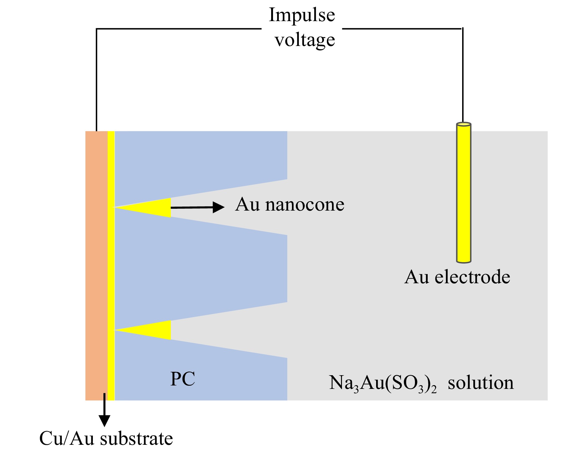
The procedure of fabricating free-standing, single gold nanocone is represented as follows: firstly, polycarbonate (PC) membranes (30 µm thickness) were irradiated with 16 MeV/u 181Ta35+ ions accelerated by the Heavy Ion Research Facility in Lanzhou (HIRFL) to induce continuous latent ion tracks. The ion fluence was 1.0×10⁸ ions/cm2. The irradiated PC membranes were then sensitized by a high-pressure mercury lamp source (MUA-165, Mejiro Genossen, Japan) at peak wavelength of 365 nm for two hours per surface. The roles of UV sensitization are increasing the track etching rate and ensuring the uniformity during etching. After sensitization, the membranes were etched by 9 mol/L NaOH solution (a mixture of methanol and water with a volume ratio of 1:1) for ~8 min. Conical pores with a maximum diameter of 1.2 µm were produced after the chemical etching. Afterwards, a thin layer of gold (~70 nm) was sputtered on one surface of PC template as a conductive layer. Before electrochemical deposition of gold nanocones, a copper layer (~10 µm) was electrodeposited using an electrolyte of 75 g/L of CuSO4·5H2O and 30 g/L of H2SO4. This composite layer of gold and copper severed as the cathode, and a 2 mm thick gold stick was used as the anode. Gold nanocones were then deposited into the conical pores by applying an impulse voltage (+1.25 V 15 s, −0.2 V 5 s) and by an aqueous solution of Na3Au(SO3)2 (75 g/L). The electrochemical deposition was closely monitored by a programmed voltage source/picoammeter (6482, Keithley, USA). The lengths of nanocones were preciously controlled to be ~20 µm via tuning the real-time deposition current and the deposition time. Finally, the membrane template was completely removed by dichloromethane (CH2Cl2) and ethanol (C2H5OH). Free-standing gold nanocones were dispersed onto silica substrates. The morphology and spectral characterizations of single nanocone were performed by utilizing scanning electron microscope (SEM, NanoSEM 450, FEI), transmission electron microscope (TEM, Tecnai F30, FEI), dark-field imaging and a broadband spectral testing system (Alpha300RAS, WITec, Germany). The plasmonic properties were analyzed by the finite-difference time-domain (FDTD, Lumerical Inc.) method. In addition, the dielectric function of gold was interpolated from the materials database (Johnson and Christy), and the size of mesh was set to 5 nm×5 nm×50 nm.
-
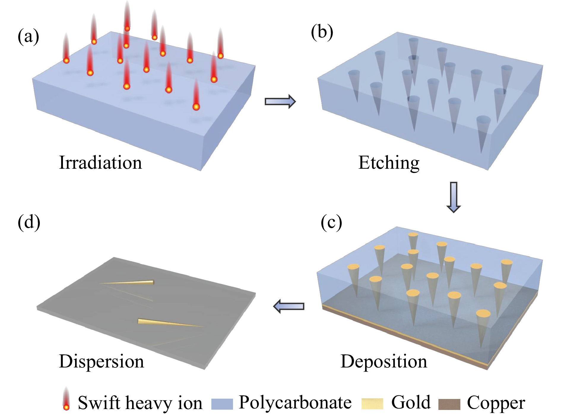
The ion-track membrane template fabrication approach has been adopted to synthesize nanostructures with excellent control for the morphology and crystallinity[20-22]. In this work, the nanocones grown in an ion-track membrane have high aspect ratio (length to diameter), and the cone tips are sharp. Also, the fabrication processes are simpler, relative to other methods such as lithography[22-24]. Figure 1 illustrates the detailed fabrication processes. Firstly, PC membranes were irradiated by swift heavy ions Fig. 1(a). According to SRIM 2013 code, the electron energy losses of incident ions in PC were estimated to be ~12 keV/nm. Such an intense energy deposition is sufficient to break multiple chemical bonds and cause crosslinks along the trajectories of ions. As the result, straight, continuous ion tracks were produced in the membranes, and the planar density of tracks can be well controlled by the incident ion fluence. After irradiation, the ion tracks were asymmetrically etched. Because the track etching rate is much higher than the volume etching rate, conical pores were drilled in the template Fig. 1(b) along the tracks. The etching time was preciously controlled to ensure that most of the conical pores were deep enough to penetrate the entire template, meanwhile the tips of pores were sharp. On the other hand, the morphologies, especially the diameter gradient of conical pores were modified by the etching solution (the concentration of NaOH and methanol). In the porous membranes, gold nanocone arrays were grown by electrochemical deposition Fig. 1(c). The length of nanocones was determined by the deposition time. The configuration of electrochemical deposition is shown in Fig. 2. The growth of the gold nanocone was initially from the tips through the nanometer size pores. An impulse voltage was applied, which resulted in small grain sizes during the growth, and uniform lengths of the nanocones. Finally, the templates were dissolved, and free-standing single nanocones were dispersed onto silica substrates Fig. 1(d). The density of dispersed nanocones on substrates was low enough to ensure that there was no crossing or overlapping between the closest nanocones during the sequential characterizations. To summarize, the ion-track membrane template method has its unique advantages and great flexibilities because all the key parameters, such as the cone length, aspect ratio and diameter gradient can be independently modified, as our previous work has demonstrated in details[23].
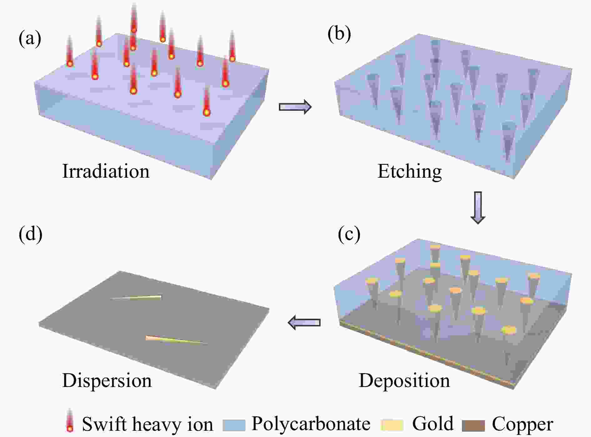
Figure 1. Schematic illustrations of the fabrication procedures of single nanocones. (a) Heavy ion irradiation on a PC membrane; (b) chemical etching to form conical pores; (c) electrochemical deposition of gold nanocones; (d) dispersion of free-standing nanocones on a substrate. (color online)

Figure 2. Schematic illustration of the electrochemical deposition process. (color online)
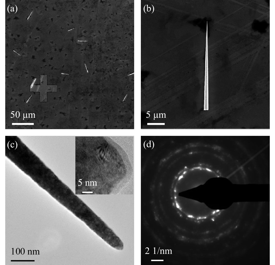
For the broadband response of a nanostructure, the morphology may have a primer impact. In this work, the morphology of single gold nanocone is characterized by electron microscopies in details. Firstly, the SEM image confirms that single nanocones are well dispersed on silica substrates. As shown in Fig. 3(a), there is no crossing between the dispersed nanocones, and the distances between nanocones are much larger than the length of nanocones. Therefore, the sequential optical characterizations are performed exactly for a single nanocone. Figure 3(b) shows the SEM image of a typical gold nanocone, which has a sharp tip and smooth contour. The length of nanocone is ~20 µm, and the maximum diameter at the bottom is ~1.2 µm. Moreover, the nanocone is perfectly conical and its diameter linearly decreases from the bottom to the tip. In order to obtain more detailed morphology and crystallinity information, TEM characterizations have been performed, especially for the tip region as shown in Fig. 3(c). It is further confirmed that the tip of nanocone is straight and sharp. The conical angle is 3.4°, and the diameter changes from 33 to 5 nm at the very end shown in the upper-left inset of Fig. 3(c) (a HRTEM image). The sharpness makes the nanocone very promising for tip enhancements. A very thin shell (~3 nm) of PC is found adheres to the tip. Because the thickness of PC layer is much smaller than the plasmon resonance wavelength, it will not affect the plasmonic spectral features of nanocones. A selected area electron diffraction(SAED) pattern suggests that the tip is polycrystalline, as shown in Fig. 3(d). The concentric patterns (Debye rings) are formed because crystals of multiple angles exist in the focused region at the tip.
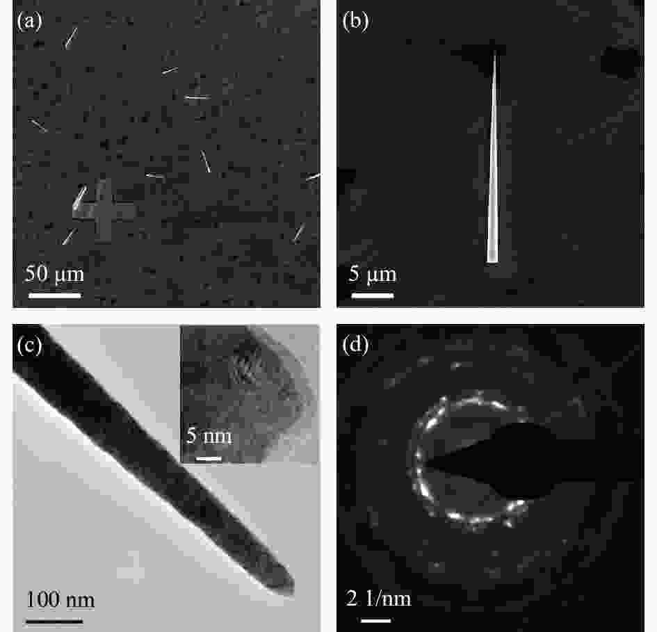
Figure 3. Electron microscopy images of the single nanocones. (a) SEM image shows the density and distribution of nanocones on a silica substrate; (b) SEM images of a typical nanocone; (c) TEM image of the nanocone tip; (d) electron diffraction pattern captured at the tip. (color online)
In order to test the broadband response of single nanocone, dark-field imaging is performed at a configuration illustrated in Fig. 4(a). A single nanocone is illuminated by a halogen lamp source with wavelength ranges from 400 to 1 200 nm through a dark-filed condenser with 20x objective and 0.8 numerical aperture(NA). According to this configuration, the scattered light from nanocone is collected by an objective in the middle, meanwhile the majority of reflected light is blocked. The dark-field image without polarization of a single gold nanocone is shown in Fig. 4(b). The scattered light origins from localized surface plasmon resonance. A reddish color is that indicates the plasmon resonance peaks are at the near-infrared region.
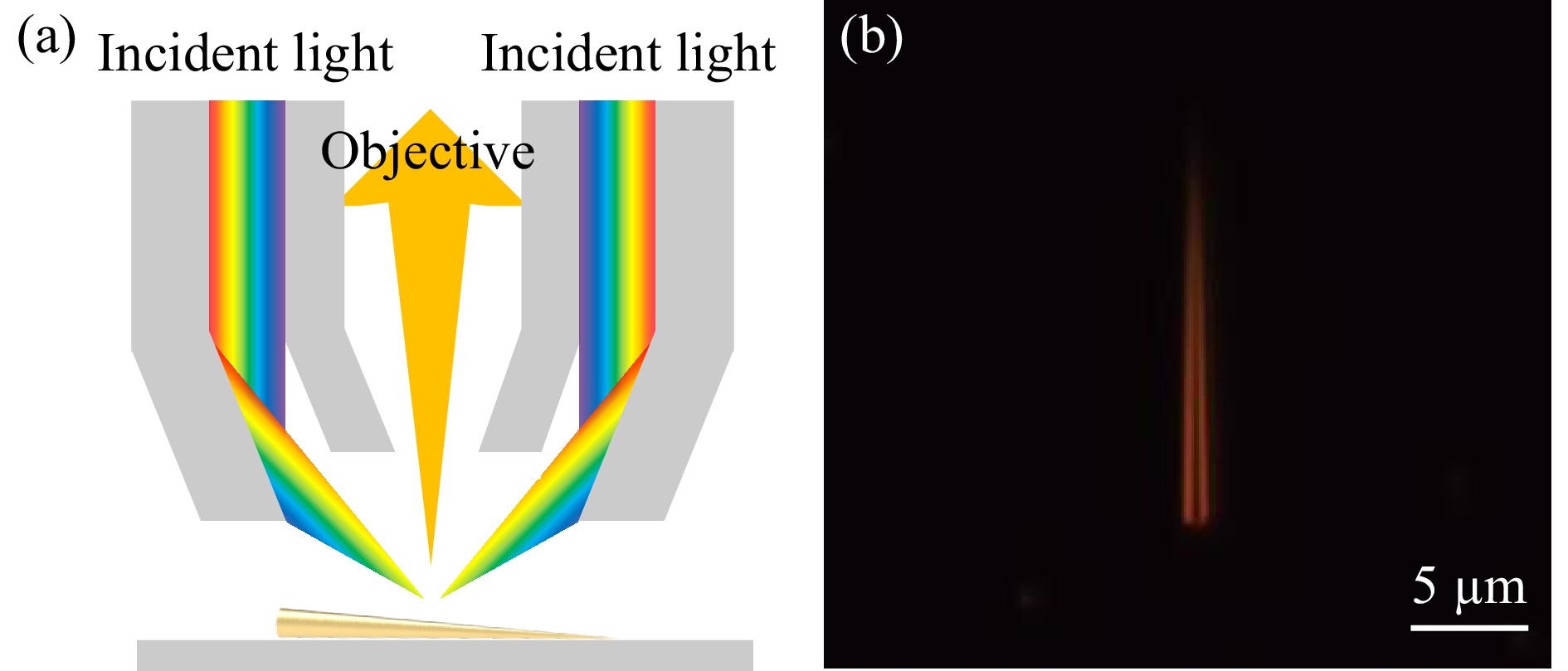
Figure 4. (a) Schematic illustration of the configuration of dark-field imaging for a single gold nanocone, (b) dark-field image captured at real-color mode. (color online)
For a perfect nanocone, its diameter decreases linearly from the bottom to the tip. Noting that surface plasmon resonance is extremely sensitive to the variation of morphology, it is expected that for our gold nanocones with very clear contour and diameter gradient along the z (longitude) axis, there will be a continuous modification for the plasmonic properties. Evidences are shown in Fig. 5(a), while the dark-field scattering spectra are collected along the z axis of a gold nanocone under non-polarized excitation. From the bottom to the tip, the scattering peak experiences a continuous redshift from 720 to 860 nm. Obviously, the surface plasmon resonances are tuned while the diameter of the nanocone changes from 1.2 µm to less than 30 nm. In addition, recently, polarized broadband light excitation draws a lot of interests. For example, it is reported that at dynamic polarization angles, it is able to tune the the surface plasmon resonance and enhance the fluorescence of organic fluorophores of metallic particles[25-28]. Therefore, for the nanocones, it is highly possible to achieve broad spectral response under polarized excitations. To verify, dark-fields scattering spectrometry were carried out with incident light at different polarization modes. The reflective spectra are plotted for 0°, 30°, 60° and 90° polarizations in Fig. 5(b~e), respectively. The results suggest that there are multiple plasmon modes for polarization angle at 0°, and the resonance peaks vary with the polarization angle. For polarization angles of 60° and 90°, the resonance modes are reduced to single. This reduction of modes is mainly due to that, the longitudinal and transverse surface plasmon resonances are tuned by polarized light excitation, because of their anisotropy. When the polarization of the incident light is parallel to the z axis of the nanocone (90°), a longitudinal plasmon mode is formed along the length of the nanocone. On the other hand, if the polarization of the incident light is perpendicular to the length of the nanocone (0°), a transverse plasmon modes is formed orthogonal to the nanocone length[28-29]. The longitudinal plasmon is highly sensitive to the aspect ratios of the structure, and the transverse plasmon is mainly tuned by the variation of diameter[30-31]. When the polarization is 90° Fig. 5(e), the longitudinal plasmon resonance dominates, and the transverse surface plasmon resonance is nearly diminished. On the other hand, when the polarization is 0° Fig. 5(b), the transverse intensity dominates. As mentioned above, the transverse plasmon intensity is as a function of the diameter. At the cone tip, where the diameter of the cone tip is small, the transverse plasmon resonance signal is weak, the longitudinal plasmon resonance is still visible in the normalized intensity spectrum. While the diameter of nanocone increases from the tip to the bottom, the transverse plasmon resonance signal increases, too. As a result, the relative intensity of longitudinal plasmon resonance keeps decreasing but it is still observable, because the maximum diameter of nanocone is ~1.2 μm, much smaller relative to the length (~20 µm). The collected spectra are in good agreement with the theoretical predictions[26, 29]. Moreover, for different polarization angles, they share a trend that the surface-plasmon-resonance induced scattering peaks are redshifted while the diameter of nanocone increases. The dark-field scattering spectra demonstrate that our single gold nanocone has achieved a broadband response in near-infrared region under different polarization modes. It also shows the potential that nanocone with well-designed morphology (for example, larger aspect ratio) may reach an even broader-band response for optical applications.
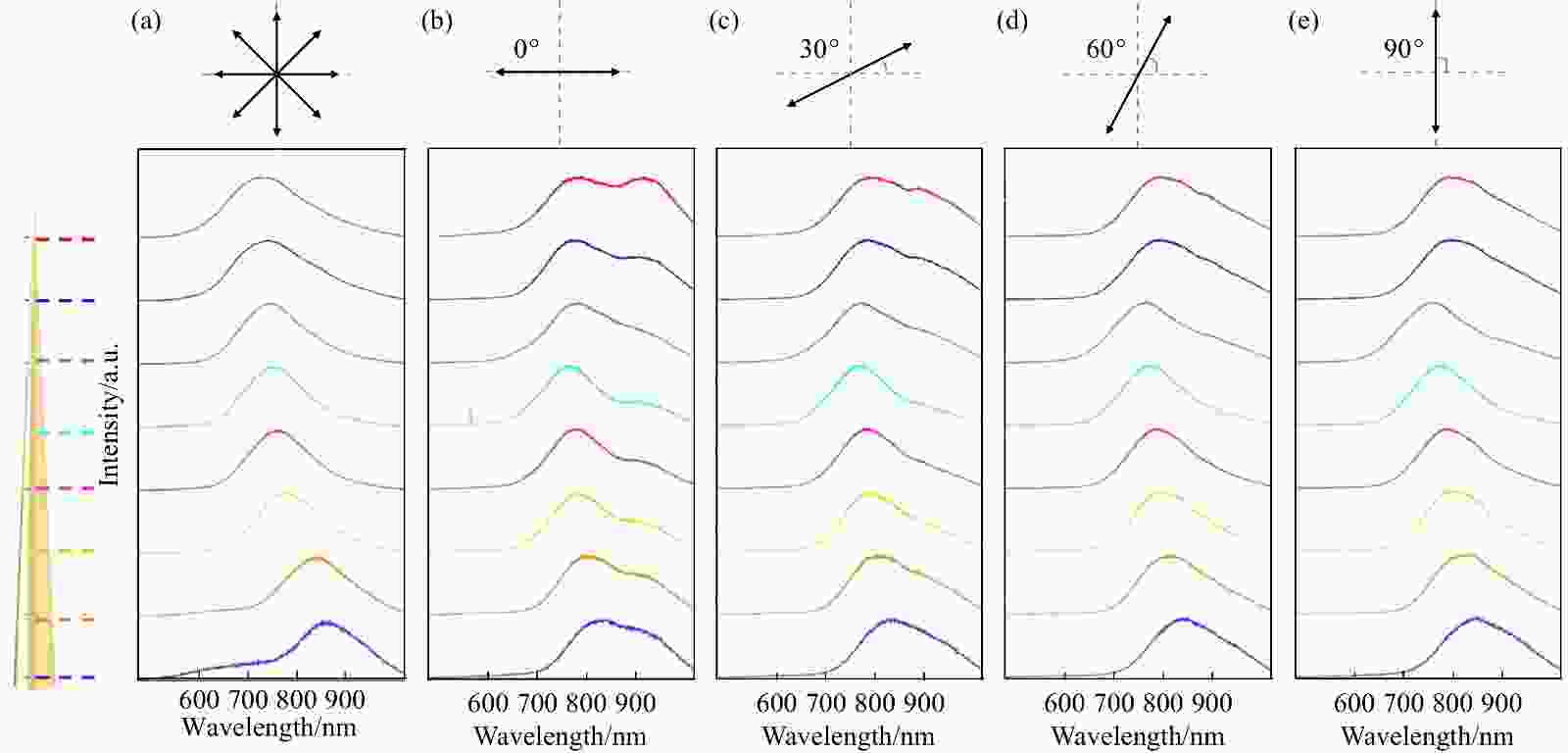
Figure 5. Dark-field scattering spectra of a single nanocone at different positions from the tip to the bottom. (a) Dark-field scattering spectra with circular polarized excitation; (b~e) dark-field scattering spectra with linearly polarized excitation at (b) 0°, (c) 30°, (d) 60°, (e) 90°. (color online)
In order to further verify the role of surface plasmon resonance to the broadband response, finite-difference time-domain (FDTD)[32-33] simulations are performed to analyze the resonance modes with spatial resolution. In the FDTD simulations, a single nanocone is illuminated by a plane wave at resonance wavelengths from 600 to 900 nm. The wave-vector is set parallel to the z axis of nanocone. The predicted electric field profiles of single nanocone peculiar dipole resonance phenomena are presented in Fig. 6. For a typical single gold nanocone with 33 nm in diameter at the tip, 1.2 μm in diameter at the bottom and a length of 20 μm, the maximum field intensity of plasmon resonance only appears at the cone tip region for 600 nm monochromatic incident light, as shown in Fig. 6(a). If the wavelength of excitation light increases, the maximum field intensity gradually moves to the bottom as shown in Fig. 6(b), 6(c) and 6(d) for excitation wavelengths of 700, 800 and 900 nm, respectively. The results are in good agreement with the spectra represented in Fig. 5, where the peaks of scattering light redshift from the cone tip to the bottom. According to the modeling and experimental results, the broadband optical response of the gold nanocones should be attributed to surface plasmon resonances, which are caused by collective oscillation of free electron gas. Also, the evolution of resonance modes confirms that linearly varied diameter is critical for modulating the density of surface plasmon.
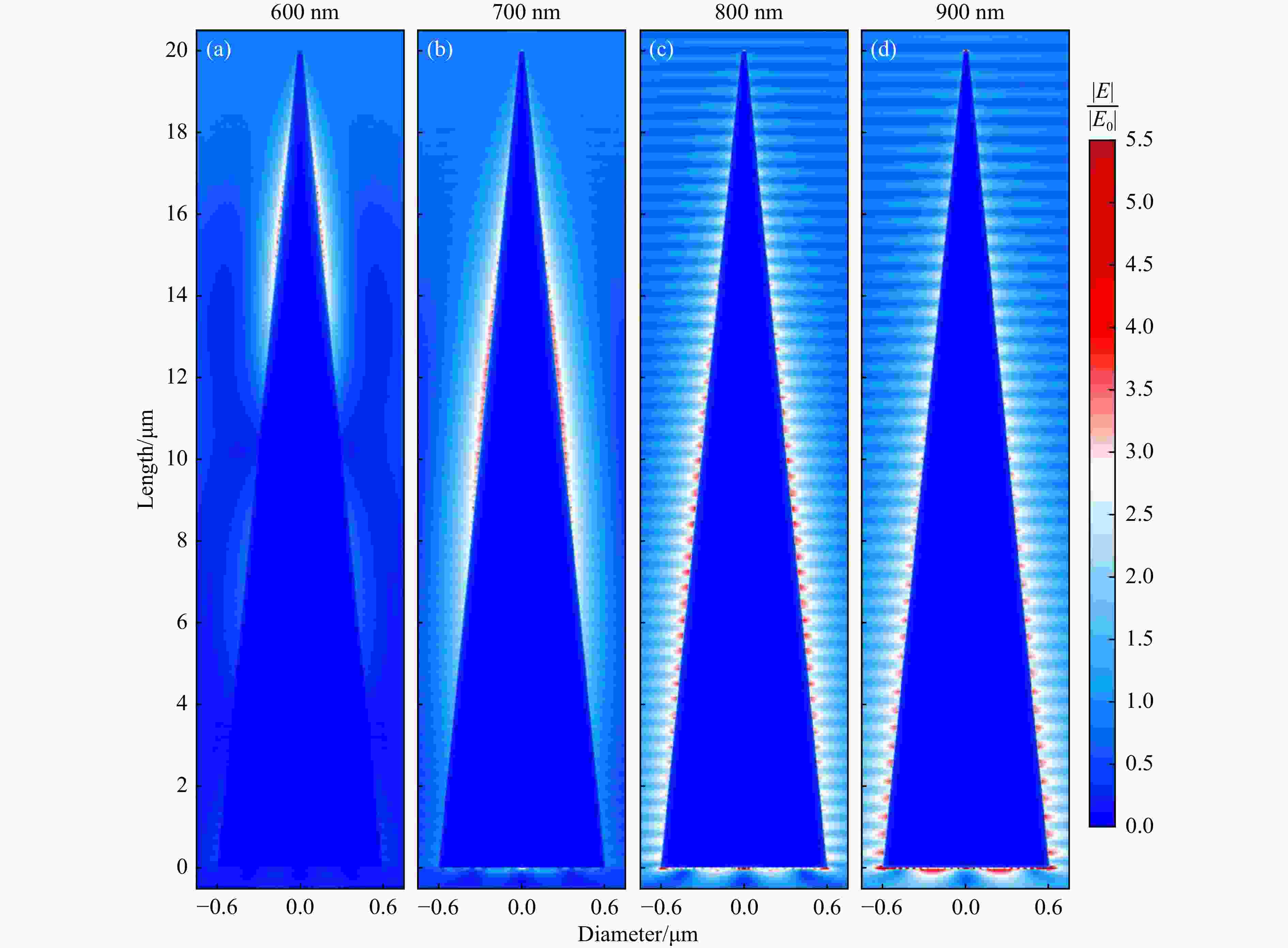
Figure 6. Electric field profiles of the single nanocone cross with different excitation wavelengths at (a) 600 nm, (b) 700 nm, (c) 800 nm, (d) 900 nm. (color online)
-
To conclude, free-standing single gold nanocones with sharp tips, high aspect ratio and smooth contour have been fabricated by an innovative ion-track membrane template method. The dark-field scattering spectra of single nanocone show wide wavelength response ranging from 600 to 1 000 nm. According to the FDTD simulations together with the measured spectra, a broad spectral response is attributed to the change of surface plasmon resonance modes. Moreover, the surface plasmon resonance is modulated by the linearly reduced diameter from the cone bottom to the tip. Notice that by taking advantages of ion-track membrane template, nanocones with well-designed morphology and varied cone angles can be fabricated in a relatively simple, precise and controllable way, we believe this attempt provides a good strategy to obtain high quality nanocones for the research of fundamental plasmonics and also for the practical applications in optoelectronics and broadband photodetections.
Acknowledgment The authors thank the HIRFL operation team for preparing 181Ta35+ SHI beams. The authors gratefully acknowledge the financial support from the National Natural Science Foundation of China(U1932210, 11975114, 12005270).
Spatially Resolved Plasmonic Properties of Single Gold Nanocone
doi: 10.11804/NuclPhysRev.40.2022015
Funds:
National Natural Science Foundation of China(U1932210, 12005270, 11975114)
- Received Date: 2022-02-28
- Rev Recd Date: 2022-04-15
- Publish Date: 2023-03-20
-
Key words:
- ion track /
- nanocone /
- broad spectral response /
- plasmonic
Abstract: Nanocones with asymmetric shapes and linearly reduced sizes possess a huge application prospect in the field of wide spectrum response. Single nanocones have great potential for the enhanced absorption/scattering and for the surface-enhanced spectroscopy caused by the excitation of surface plasmon. In this work, free-standing single gold nanocones with gradient diameter were fabricated by swift heavy ion irradiation on polymeric templates, followed by latent track etching and electrodeposition processes. The morphology and structure characterizations were performed, included scanning electron microscopy, transmission electron microscopy and optical dark-field imaging. Further dark-field scattering spectrometry results showed that the single gold nanocones have broadband response and multiple polarization modes. In addition, FDTD (the finite-difference time-domain) simulations revealed the mechanisms beneath the broadband plasmonic responses, which are attributed to the variation of surface plasmon resonance modes as a function of the gradually changed diameters of gold nanocone. This work provides an innovative method for the fabrication of high-quality gold nanocones, and also provides systematic theoretical and experimental evidence for the in-depth study of the broadband response properties of single metallic nanocones.
| Citation: | Ran HUANG, Wentao WANG, Fangfang XU, Yuhui HU, Jiaming ZHANG, Yonghui CHEN, Haizhou XUE, Jinglai DUAN. Spatially Resolved Plasmonic Properties of Single Gold Nanocone[J]. Nuclear Physics Review, 2023, 40(1): 99-105. doi: 10.11804/NuclPhysRev.40.2022015

|
 甘公网安备 62010202000723号
 DownLoad: