


-
低温高密核物质测量谱仪(CSR External-target Experiment, CEE)建成后将是我国第一台GeV能区自主研制的大型核物理实验装置,如图1所示,该实验装置包含了飞行时间探测器、束流位置探测器、起始时间探测器等多种探测器[1]。

Topmetal-CEE是一款顶层金属开窗的硅像素芯片[2],位于束流探测器的前端电子学芯片中,用于测量入射束流的位置和时间信息。然而,由于探测器中前端电子学与后端电子学通过长达几米的同轴电缆连接[3],供电系统提供的3.3 V电源电压到达Topmetal-CEE芯片时会产生较大压降,最低可降至2.5 V,如果没有片上供电系统为芯片提供稳定的电源电压,读出电子学系统将无法工作,因此,探测器的供配电系统中采用DC-DC变换器(DC-DC Converter)与LDO(Low-Dropout Regulator, LDO)电路进行供电[3] 。为了满足像素探测灵敏区的要求,探测器中有多个Topmetal-CEE芯片交错排列,同时需要多个LDO电路对这些芯片供电,每个LDO的静态功耗不超过10
$ {\text{μA}} $ ,这对LDO功耗和面积提出了较高的设计要求。传统LDO的片外电容通常在${\text{μF}}$ 量级, LDO内部需要使用大尺寸晶体管驱动输出电容,这使得电路面积较大,不适用于Topmetal-CEE芯片中,因此设计了一种集成于Topmetal-CEE内部的无片外电容LDO电路,用于为低压模拟电路以及数字模块提供1.2 V电源电压。无片外电容LDO作为数模混合电路的供电电源使用时,负载电压或电流变化会影响LDO供电电压稳定性,以LDO负载电流变化为例,Topmetal-CEE中低压模块工作所需最大电流可达十几毫安,如果负载突然从LDO抽取大电流,将导致LDO提供的输出电压小于1.2 V,影响Topmetal-CEE芯片的正常工作。此外,LDO输入电压变化也会影响其输出电压,所以LDO的功耗、负载瞬态响应和线性调整率等性能是设计的关键。目前,现有的无片外电容低压差线性稳压器(Output-Capacitorless Low-Dropout Regulator, OCL-LDO)结构大多基于翻转电压跟随(Flipped Voltage Follower, FVF)结构[4-8],因为这种结构可以通过负反馈实现自我调节,具有较高的稳定性。基于FVF结构的LDO电路如图2所示,功率管为
$ {M_{\text{P}}} $ ,功率管的栅极等效电容为$ {C_{{\text{par}}}} $ ,输入和输出电压分别为$ {V_{{\text{IN}}}} $ 和$ {V_{{\text{OUT}}}} $ ,$ {V_{{\text{BIAS}}}} $ 、$ {V_{{\text{SET}}}} $ 以及$ {I_{{\text{BIAS1}}}} $ 、$ {I_{{\text{BIAS2}}}} $ 表示偏置电压与偏置电流。电路中的共栅放大器$ {M_{{\text{C1}}}} $ 与$ {M_{{\text{C2}}}} $ 形成一个折叠误差放大器,由$ {M_{{\text{C1}}}} $ 的源级检测LDO的输出电压并将其与电压$ {V_{{\text{SET}}}} $ 进行比较,比较结果被$ {M_{{\text{C2}}}} $ 放大,然后输出至功率管的栅极处,根据瞬时极性法,$ {M_{\text{P}}} $ 与折叠误差放大器构成负反馈,从而实现闭环电压调节。
提出的LDO电路基于FVF结构实现,采用单个密勒电容进行补偿,相比嵌套密勒补偿节省了功耗和面积[9]。为防止低功耗时的大信号响应限制负载瞬态响应的速度,使用电压峰值检测电路检测输出电压变化,偏置电路根据负载的电压变化调整偏置电流,达到节省功耗的目的[10-11]。由于亚微米器件比长沟道器件沟道长度调制效应更严重,负载调节性能更差,所以设计的LDO在FVF结构的基础上增加了一级同相放大电路,并且采用class-AB结构作为输出级,增强了LDO电路的负载调节能力[5] ,减小了过冲和下冲的幅度,同时提高了环路增益和带宽。尽管该LDO属于模拟电路,辐射对其影响小,但为了保证电路的高性能,该LDO电路的功率管选择p管,因为p管具有抗总剂量效应[12],受辐射后阈值电压增大,泄露电流减小。
-
无片外电容低压差线性稳压器在深亚微米工艺中的设计重难点在于:1) 增强环路增益以便更好地进行负载调节;2) 优化静态电流以节省功耗;3) 使片上电容尽可能小,从而减小芯片面积[5]。FVF结构具有较小的静态电流,但瞬态响应速度较慢,此外,其误差放大器只采用了简单的折叠电路,这导致LDO的负载调整性能较差。为了克服上述问题,设计了一种采用130 nm CMOS技术实现的、基于FVF结构和单个电容补偿的OCL-LDO,该电路实现了高稳定性、快速瞬态响应和较小过冲,可驱动大电容负载,而且无需片外电容。具体结构如图3所示,输入和输出电压分别为
$ {V_{{\text{IN}}}} $ 和$ {V_{{\text{OUT}}}} $ ,电路结构主要包括电压峰值检测电路(也可称为动态偏置电路,包括:$ {M_{{\text{B1}}}} $ 、$ {M_{{\text{B2}}}} $ 、$ {M_{{\text{B3}}}} $ 、$ {R_1} $ 、$ {C_1} $ ),控制电压$ {V_{{\text{SET}}}} $ 产生电路(${M_{01}}{ \sim }{M_{05}}$ )以及功率管$ {M_{\text{P}}} $ 。误差放大器则由折叠共栅放大器(${M_{11}}{ \sim }{M_{16}}$ )和同相增益级(${M_{21}} \sim{M_{24}}$ )两部分构成,$ {C_{\text{m}}} $ 为补偿电容,$ {C_2} $ 为滤波电容。与图2相比,误差放大器中加入了同相增益级提高环路增益,从而增强负载调节性能。同相增益级还有另一个重要的优点,即增加FVF结构中功率管栅极电压的动态范围,$ {M_{\text{P}}} $ 的最小栅极电压仅为$ {M_{23}} $ 的饱和电压,增大的$ {V_{{\text{sg}}}} $ 使得$ {M_{\text{P}}} $ 可以在更小的尺寸下流过大电流。位于$ {M_{15}} $ 漏极和$ {V_{{\text{OUT}}}} $ 之间的密勒电容$ {C_{\text{m}}} $ 用于提高环路稳定性,因为采用的是深亚微米晶体管,LDO输出结点和同相增益级输入结点的极点频率都不在低频处,如果没有补偿电容,则LDO的输出电压容易发生振荡[5]。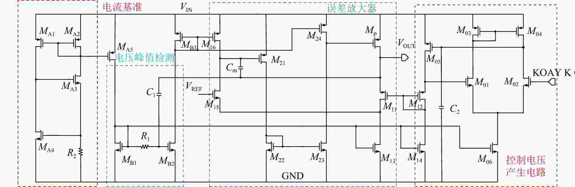
-
电压峰值检测电路实质上是一个动态偏置电路,如图4所示,偏置电路主要由
$ {M_1} $ 和$ {M_2} $ 构成的电流镜组成,$ {I_1} $ 和$ {I_2} $ 分别为电流镜输入电流和输出电流,在其中加入两个无源器件$ {R_1} $ 和$ {C_1} $ 就能实现动态偏置。当电容$ {C_1} $ 检测到输出电压突变时,$ {M_2} $ 的栅极电压随之改变,流过$ {M_2} $ 的电流$ {I_2} $ 发生改变,加快对${C_{{\text{par}}}}$ 的充放电速度,从而起到增强瞬态响应的效果[11]。在稳态时,$ {V_{{\text{PULSE}}}} $ 是一个常数,所以$ {V_{{\text{SG2}}}} $ 由$ {V_{{\text{SG1}}}} $ 决定,此时$ {I_1}{\text{ = }}{I_2} $ 。当$ {V_{{\text{PULSE}}}} $ 的幅值突然由低变为高(假设变化量为$ \Delta V $ ),$ {R_1} $ 和$ {C_1} $ 组成的高通滤波电路会使突变的电压耦合到$ {M_2} $ 的栅极,使得$ {I_2} $ 增加$ \Delta {I_2} $ 。需要注意的是,$ {R_1} $ 应该选择较大的值,这是为了隔离$ {M_1} $ 和$ {M_2} $ ,防止$ {V_{{\text{SG}}1}} $ 受到影响。对$ {M_2} $ 的电流变化进行数学推导:
式中:
$ {\mu _{\text{n}}} $ 表示n型晶体管的电子迁移率;$ {C_{{\text{ox}}}} $ 表示单位面积的栅氧化层电容;$ {V_{{\text{TH}}}} $ 表示晶体管的过驱动电压;$ W $ 与$ L $ 代表晶体管的宽度与长度,将式(1)整理后可以得到表达式:从式(2)可看出
$ {M_2} $ 的宽长比越大,瞬态电流也就越大,并且$ {C_1} $ 越小,电压峰值检测电路越敏感。 -
误差放大电路的拓扑结构如图5所示,由折叠共栅放大器(
${M_{21}}{ \sim }{M_{24}}$ )和同相放大器($ {M_{11}}{ \sim }{M_{16}} $ )构成。以像素芯片抽取的电流突然增大为例,此时LDO的功率管$ {M_{\text{P}}} $ 来不及提供足够大的电流,导致LDO输出电压下降,输出电压的变化经过误差放大器后被放大,$ {M_{\text{P}}} $ 的栅极电压下降,过驱动电压增大,$ {M_{\text{P}}} $ 管提供的电流增多,输出电压回升。误差放大器中的同相放大器具有增益增强的作用,因为误差放大器的增益越大,负载瞬态响应越强。同相放大器的输出级可看成一个class-AB结构[13],用于增强误差放大器的驱动能力,节省功耗。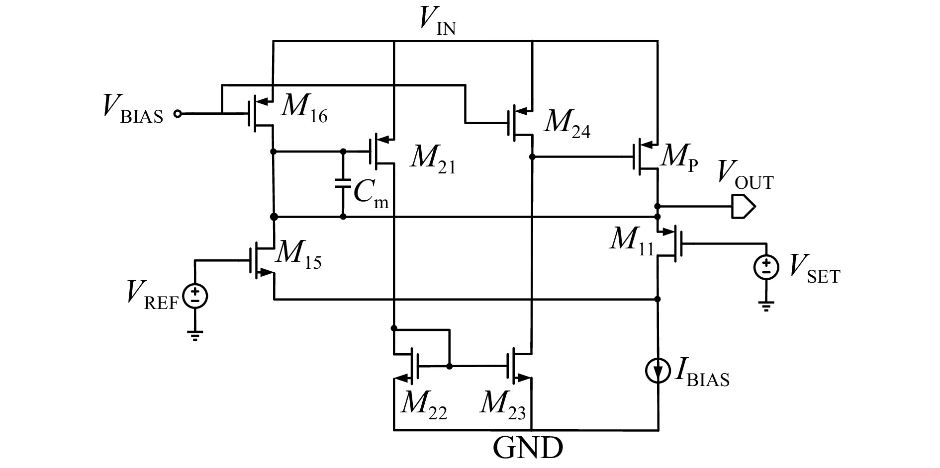
-
如果不采用补偿策略,由于130 nm晶体管的寄生电容和晶体管的漏极电阻较小,图2所示的LDO没有低频主极点,稳定性较差。为了解决这一问题,采用了密勒补偿技术,即在同相增益级的输入端和功率管的输出端之间加了一个补偿电容[8-9, 14]。在华虹宏力130 nm工艺中,由于功率管的栅极和漏极之间的寄生电容较小,并且在不同的负载电流时,
$ {M_{\text{P}}} $ 的本征增益也有限,所以功率管$ {M_{\text{P}}} $ 的寄生电容$ {C_{{\text{GD}}}} $ 的密勒效应可以忽略不计。图6给出了图2所示LDO结构的等效小信号模型,其中$ {g_{{\text{m}}i}} $ 、$ {R_{{\text{o}}i}} $ 和$ {C_{{\text{o}}i}} $ 分别代表第$ i $ 级的等效跨导、等效输出电阻和寄生电容,$ {g_{{\text{mp}}}} $ 代表功率管的等效跨导,图中的$ {C_{\text{m}}} $ 为补偿电容,${R_{\rm{OUT}}}$ 表示输出电阻,${C_{\rm{OUT}}}$ 表示LDO输出端的总寄生电容,它包括LDO自身的寄生电容、电源走线和负载电路的寄生电容。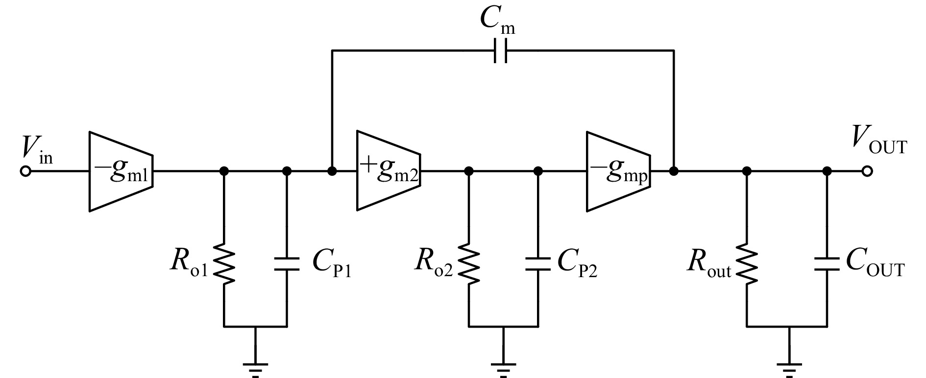
由图5得出LDO整体电路的传输函数为
上述公式中,
$ {A_{{\text{dc}}}} $ 为低频开关增益;${P_{{{ - 3{\rm{dB}}}}}}$ 为系统的主极点;${\omega ^{}_{{\text{GBW}}}}$ 表示环路的单位增益带宽;它们的表达式分别为$ {A_{{\text{dc}}}} = {g_{{\text{m}}1}}{g_{{\text{m}}2}}{g_{{\text{mp}}}}{R_{{\text{o}}1}}{R_{{\text{o}}2}}{R_{{\text{OUT}}}} $ ,${P_{{{ - 3{\rm{dB}}}}}} = \frac{1}{{{C_{\text{m}}}{R_{{\text{o}}1}}{g_{{\text{m}}2}}{g_{{\text{mp}}}}{R_{{\text{o2}}}}{R_{{\text{OUT}}}}}}$ ,${\omega^{} _{{\text{GBW}}}} = {A_{{\text{dc}}}} \cdot {P_{ - 3 {\text{dB}}}} = \frac{{{g_{{\text{m}}1}}}}{{{C_{\text{m}}}}}$ 。根据式(5)的传输函数可以看出,系统具有两个次极点和两个零点。当$ {C_{\text{m}}} $ 比较小且${g^{}_{{\text{mp}}}}$ 比较大时,零点在高频处,可以忽略不计。所以式(3)也可以写成:为了使整个系统符合实际电路的情况,
${C_{{\text{OUT}}}}$ 应满足如下关系:其中
$ {R_{{\text{OUT}}}} \approx \frac{1}{{\lambda {I_{{\text{OUT}}}}}} $ ($ \lambda $ 为沟道长度调制系数),所以式(7)可写成:式中:
${\mu^{} _{\text{p}}}$ 表示p型晶体管的电子迁移率;$ {I_{{\text{OUT}}}} $ 表示输出电流。根据上述条件,式(3)可以表示为其中次级点
$ {P_2} $ 与$ {P_3} $ 的表达式为为了使LDO有较好稳定性,
$ {P_2} $ 和$ {P_3} $ 应满足如下条件:根据理论分析,
$ {P_2} $ 至少大于$2{\omega^{} _{{\text{GBW}}}}$ ,这样可以保证整个系统的稳定性[14]。设计的LDO环路的单位增益带宽约为1.185 MHz,第二个极点
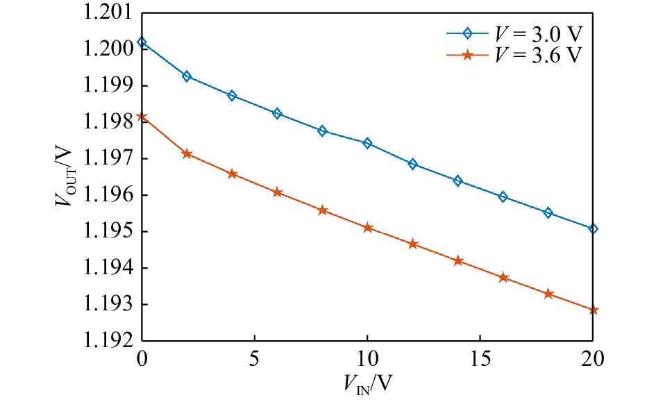
$ {P_2} $ 的位置位于10 MHz处,第二个极点的频率是单位增益带宽的8.44倍,表明该系统具有很高的稳定性。图7为LDO环路增益与相位曲线的仿真结果,仿真时的输入电压分别为2.5,3.0,3.6 V,负载电流为20 mA,负载电容为100 pF。仿真结果表明,当输入电压变化时,LDO环路性能相差极小,图7中的低频增益最大仅相差1.3 dB,且在不同工艺角下,环路增益均大于75 dB,相位裕度大于75°,设计的LDO结构具有较好的稳定性。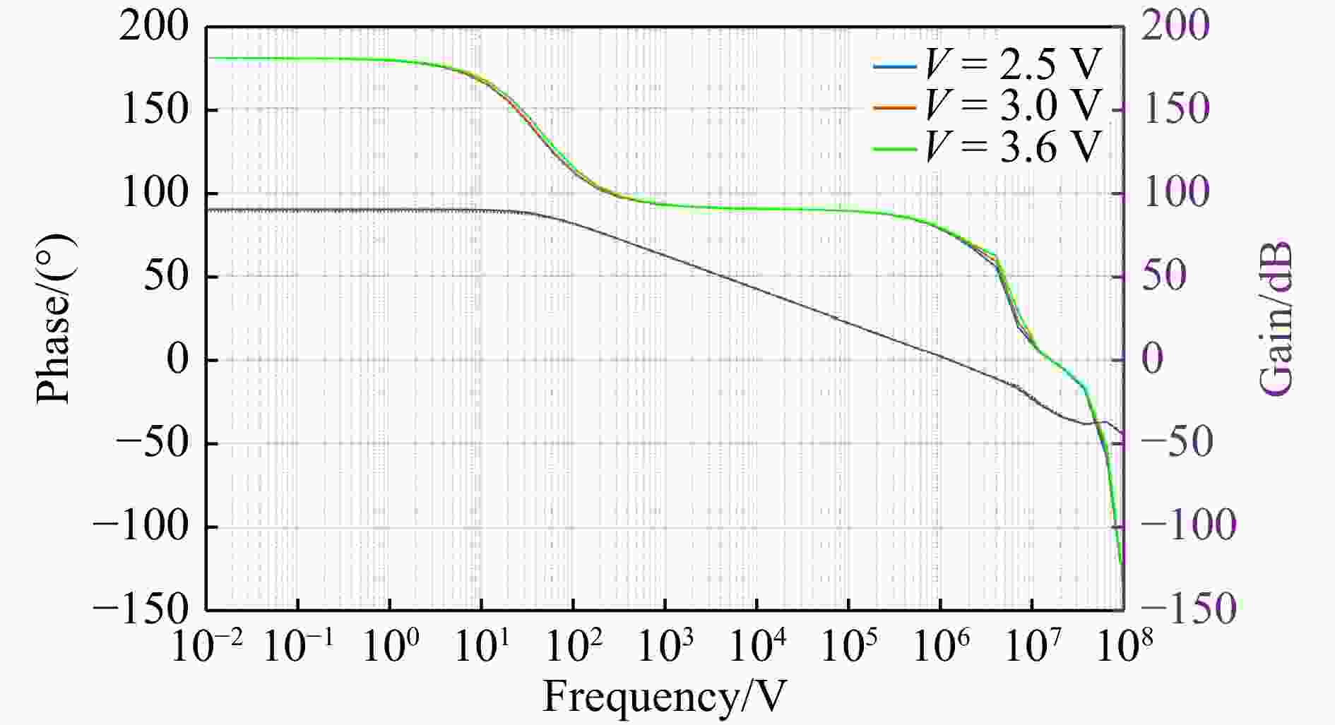
-
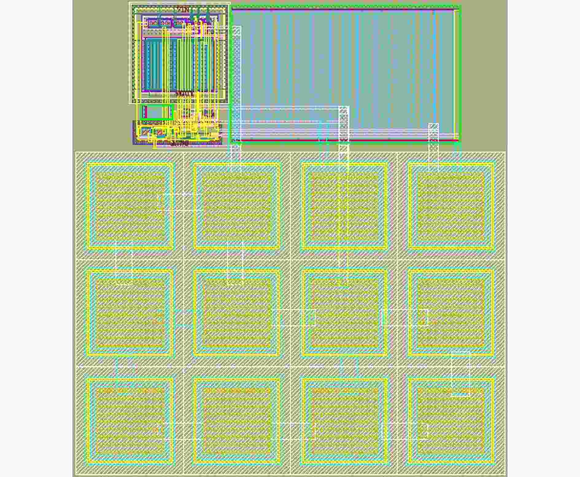
设计的LDO采用国产GSMC 130 nm CMOS工艺,整个版图的面积大小仅103.5 μm×95.2 μm。如图8所示,其中面积占比最大的部分是补偿电容,位于版图下方,其次是偏置电路中的电阻,位于右上方,CMOS晶体管位于版图左上侧,其外围是一圈保护环,保护环不仅可以消除单粒子闩锁的影响,还能够抗总剂量效应[12] ,减小辐射的影响。
-
设计的LDO的输出电压为1.2 V,输入动态范围为2.4~3.6 V。LDO的静态电流为8.5
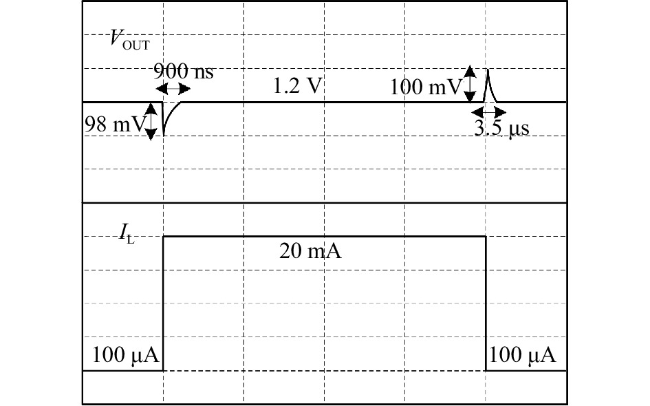
$ {\text{μA}} $ ,最大负载电流为20 mA。版图设计完成后,对LDO进行性能仿真(所有仿真均在负载电容为100 pF下进行),线性调整率如图9所示,仿真结果表明,在负载电流为0 mA和20 mA时,线性调整率分别为3.2,3.3 mV/V。负载调整率如图10所示,在输入电压为3 和3.6 V 时的负载调整率分别为256, 266$ {\text{μV}} $ /mA。LDO的负载瞬态响应波形见图11,当输出电流在100$ {\text{μ A}} $ 至20 mA之间跳变时,过冲和下冲电压约为100 mV,恢复时间分别为3.5$ {\text{μs}} $ 、900 ns。LDO在各工艺角下仿真的输出电压情况如表1(输入电压为2.5 V,负载为100 pF),由图可知输出电压在ss工艺角下最小,在ff工艺角下达到最大,这是由于ss工艺角下阈值电压高,功率管的源漏电压大,导致输出电压偏低,ff工艺角下阈值电压低,功率管的$ {V_{{\text{ds}}}} $ 较小,因此输出电压偏高,但误差都在芯片可正常工作范围内。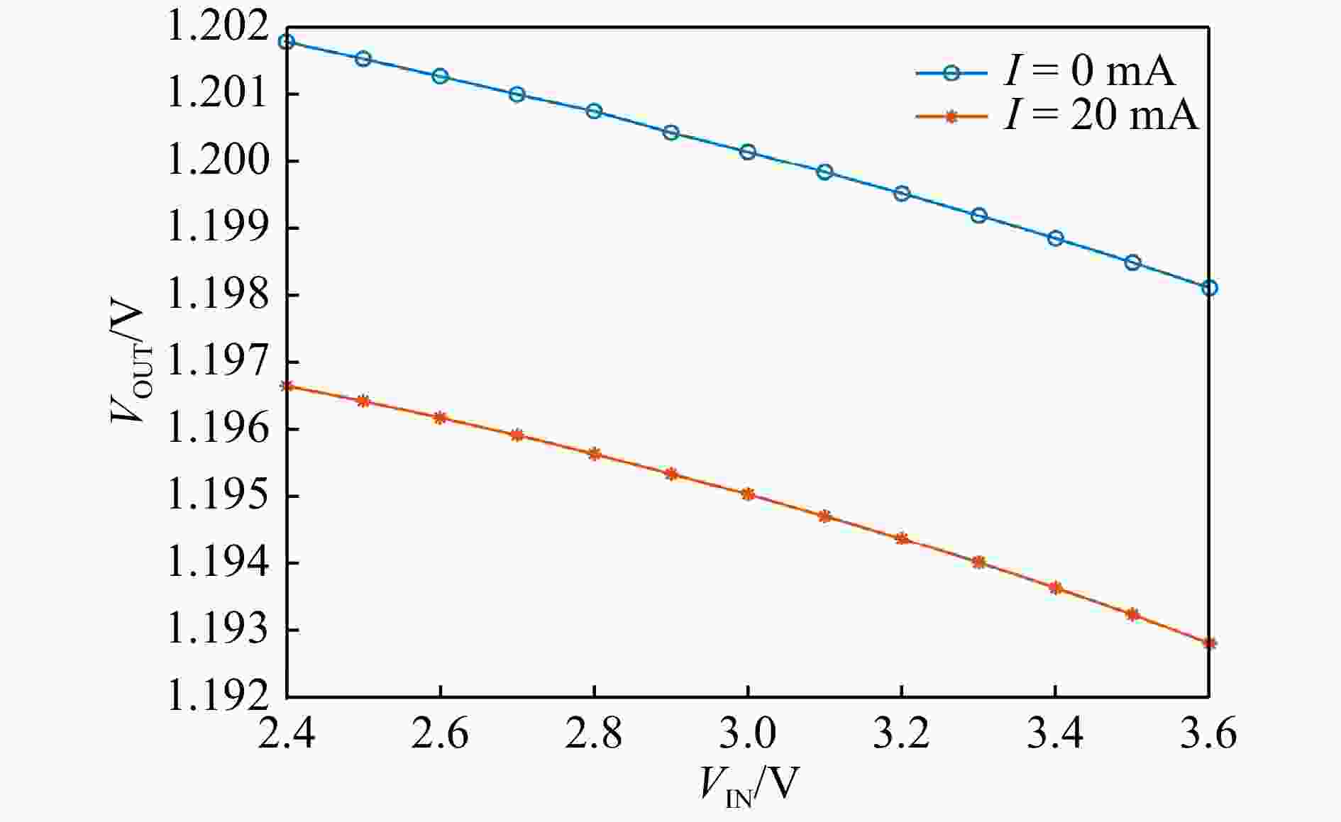
温度(°C) 负载电流为100 $ {\text{μA}} $时
的输出电压/V负载电流为20 $ {\text{mA}} $时
的输出电压/Vss tt ff ss tt ff −40° 1.199 1.201 1.206 1.195 1.197 1.201 27° 1.199 1.201 1.207 1.194 1.197 1.201 125° 1.195 1.199 1.205 1.189 1.193 1.199 负载调整率 −0.96%~+0.58% 表2为本文与其他已发表文献设计的无片外电容LDO的主要性能参数对比,表中的稳定时间、过冲与下冲电压等性能参数是输入电压为2.5 V,负载为100 pF时的后仿真结果。由表2可看出与文献[15-17]对比,设计的LDO具有最低的静态电流,过冲电压也较小,因此设计的无片外电容LDO在低功耗下依然具有较强的瞬态响应。
-
为了达到束流探测器中读出电子学芯片对LDO小面积和低功耗的高要求,设计了一款基于FVF结构、由单个密勒电容补偿的低压差线性稳压器。在设计中采用了动态偏置在减小静态功耗的同时增强负载瞬态响应。在误差放大器中,输入级采用折叠共栅放大器提高带宽,并增加同相增益级提高增益,减小输出电压的过冲和下冲,而且只通过单个电容补偿便达到了较好的稳定性。仿真结果表明,在负载电容为100 pF、负载电流20 mA时,线性调整率为3.3 mV/V,输入电压为3 V时最大恢复时间为3.5 μs,静态功耗8.5 μA,设计的LDO在功耗与瞬态响应方面具有较大优势,适合为复杂的探测器系统芯片供电。
A Low Power and Strong Transient Response LDO Circuit
doi: 10.11804/NuclPhysRev.40.2022071
Funds:
General Program of National Natural Science Foundation of China(12075100)
- Received Date: 2022-06-16
- Rev Recd Date: 2022-08-15
- Available Online: 2023-12-07
- Publish Date: 2023-09-20
-
Key words:
- CEE /
- readout electronics /
- lip voltage follower(FVF) /
- low dropout linear regulator(LDO)
Abstract: A large number of pixel sensor chips are integrated on the beam detector in CEE experiment, in order to provide stable power voltage for these chips, and meet the high requirements of silicon pixel chips for small area and low power consumption of power supply circuit, a low voltage differential linear regulator(Low-dropout regulator, LDO) circuit compensated by a single Miller capacitor is realized in 130 nm CMOS process of GSMC. The proposed LDO based on the flip voltage following(Flipped Voltage Follower, FVF) structure which can achieve high stability, fast transient performance and ultra-low power consumption when the load current changes rapidly, and does not require off-chip capacitance when using small transistors. The experimental results show that the structure can drive a capacitive load of 0~100 pF when the load current is 20 mA, the line regulation is 3.3 mV/V, the quiescent current is 8.5 μA, and the layout area is only 103.5 μm×95.2 μm, which is suitable for highly complex detector system chips.
| Citation: | Jiajia LIU, Qingwen YE, Ping YANG. A Low Power and Strong Transient Response LDO Circuit[J]. Nuclear Physics Review, 2023, 40(3): 433-438. doi: 10.11804/NuclPhysRev.40.2022071

|


 甘公网安备 62010202000723号
 DownLoad:


