


-
随着航天航空技术、核技术以及军事技术的发展,具有高功率、高效率、低体量并适用于高温、强辐射环境的电力电子系统得到了广泛的应用[1-2]。然而,传统的Si基功率器件由于其本身材料属性的限制,在大功率器件方面的应用受到诸多限制。
SiC材料具有高击穿电场、高热导率、高电子密度和高电子迁移率等特点,因此,SiC器件在大功率应用领域具有更明显的优势。相比于Si基功率器件,在航空航天电子设备中使用的SiC基功率器件能明显地减轻电子设备整体重量,有效提升卫星、空间站的探测器效率和有效载荷[1-7]。特别是,SiC双沟槽MOSFET器件(SiC double-trench MOSFET, SiC DT-MOS)更好地平衡了临界击穿电压和导通电阻等特性,在航空动力电力系统中具有良好的适用性[8]。
SiC基MOSFET器件易受宇宙射线中的高能重离子的影响,导致灾难性单粒子烧毁效应(Single-Event Burn-out, SEB)[1-8]。Zhou等[8]利用TCAD模拟研究了SiC DT-MOS器件的SEB过程,当线性能量转移(Linear Energy Transfer, LET)为1 pC/μm时,发生SEB的阈值电压为70 V,发生单粒子栅穿效应(Single-Event Gate Rupture, SEGR)的阈值电压为20 V,结果表明SiC DT-MOS器件的抗辐射性能较差,可能会影响其在空间应用中的安全运行;Zhang等[9]利用TCAD和蒙特卡罗程序模拟计算了SiC MOSFET器件的SEB灵敏度,结果表明:大电流与强电场共存时,器件局部区域的晶格温度超过SiC的熔点;Ball等[10]采用TCAD程序模拟计算了由重离子诱导高压SiC MOSFET器件和SiC肖特基势垒二极管的单粒子烧毁效应,在确定漏源电压和入射离子能量的条件下,重离子入射导致器件内部电场达到或超过雪崩击穿所需的临界电场,可能导致器件发生单粒子烧毁。综上模拟结果,SiC基MOSFET器件在重离子辐照条件下易发生损伤效应,然而模拟过程中并未考虑碰撞电离在器件内部的影响以及晶格的自热效应等过程。
本文采用TCAD程序,考虑晶格自热效应,开展SiC双沟槽MOSFET器件的单粒子烧毁效应模拟仿真研究,模拟计算重离子入射条件下漏源电压对SiC双沟槽MOSFET器件的单粒子烧毁效应的影响,给出了强电场对碰撞电离的影响以及晶格温度升高原因。
-
利用TCAD仿真工具构建了SiC双沟槽MOSFET器件模型,截面示意如图1所示。外延层厚度为9 μm,掺杂浓度为3×1015 cm−3,用于器件单粒子效应加固的缓冲层厚度为1.5 μm,掺杂浓度为3×1017 cm−3,其击穿特性曲线如图2所示,击穿电压为1 512 V。因此,本次模拟选取的偏置电压均低于1 512 V,器件的详细参数如表1所列。

参数 值 单个器件宽度/μm 5.7 N-漂移区深度/μm 9 N-漂移区掺杂浓度/cm−3 3×10¹⁵ 衬底深度/μm 150 源/栅极沟槽深度/μm 1.55 源/栅极沟槽宽度/μm 2 栅氧化层厚度/nm 50 N+源极深度/μm 0.2 N+源极和衬底掺杂浓度/cm−3 1×10¹⁹ N+缓冲区深度/μm 1.5 N+缓冲区掺杂浓度/cm−3 3×10¹⁷ P-基区深度/μm 0.5 P-基区掺杂浓度/cm−3 2×10¹⁷ P型区域深度/μm 1.8 P型区宽度/μm 1.35 P型区掺杂浓度/cm−3 2×10¹⁸ 本论文采用TCAD软件开展SiC双沟槽MOSFET器件的单粒子烧毁效应模拟研究,根据Mcpherson等[11]对SiC材料中与电热效应相关的导热系数、热阻和热容参数进行修正,热导率、热阻和热容分别表示为
其中:T为SiC的晶格温度;
$\alpha _1 $ =−1.882 2×10⁻¹ cm∙K/W;$\beta_1 $ =1.636 7×10⁻³ cm/W;$\gamma_1 $ =−1.694 1×10⁻²⁰ cm/(W∙K) ;$\alpha _2 $ =1.577 8×100 J/(K∙cm3) ;$\beta_2 $ =3.533 2×10⁻³ J/(K2∙cm3);$\gamma_2 $ =−1.544 7×10⁻⁶ J/(K3∙cm3);μ2=2.605 2×10⁻¹⁰ J/(K4∙cm3)。 -
采用器件仿真软件Sentaurus TCAD[8]开展重离子辐照SiC双沟槽MOSFET器件的SEB效应模拟计算。其中采用了重离子辐照模型,具体原理如下:当重离子穿透一个半导体器件时,它会损失能量,并沿入射径迹产生一系列的电子-空穴对,这些额外的电子和空穴可能会形成足够大的电流来影响器件的运行状态。由重离子引起的电子-空穴对的生成率表示为
其中:R(w,l)和T(t)分别为描述电子空穴对产生率的时空变化的函数;GLET(l)是线性能量转移(LET)[12-14]的产生密度;l表示离子径迹长度,设置为11 μm,其长度贯穿该器件的寄生晶体管,使寄生晶体管更易导通;w为离子径迹半径,决定电子空穴对的产生范围,本工作离子径迹半径w设置为0.03 μm[8]。LET值设置为0.1 pC/μm[8]。重离子入射产生的电子-空穴对数在4 ps时达到峰值[8]。
值得注意的是,二维模拟不同于三维模拟,离子入射产生的电子空穴对在器件中的空间分布是薄片状而非圆柱状,因此,本文为定性而非定量研究。本模拟工作基于禁带宽度变窄(BGN)模型、肖克利-里德霍尔(SRH)复合模型、俄歇复合模型、雪崩击穿模型等物理模型[2],还考虑了SiC材料的不完全电离和各向异性[15],对于晶格温度的计算,使用了热力学模型[15],用于计算器件内部非均匀分布的晶格温度。
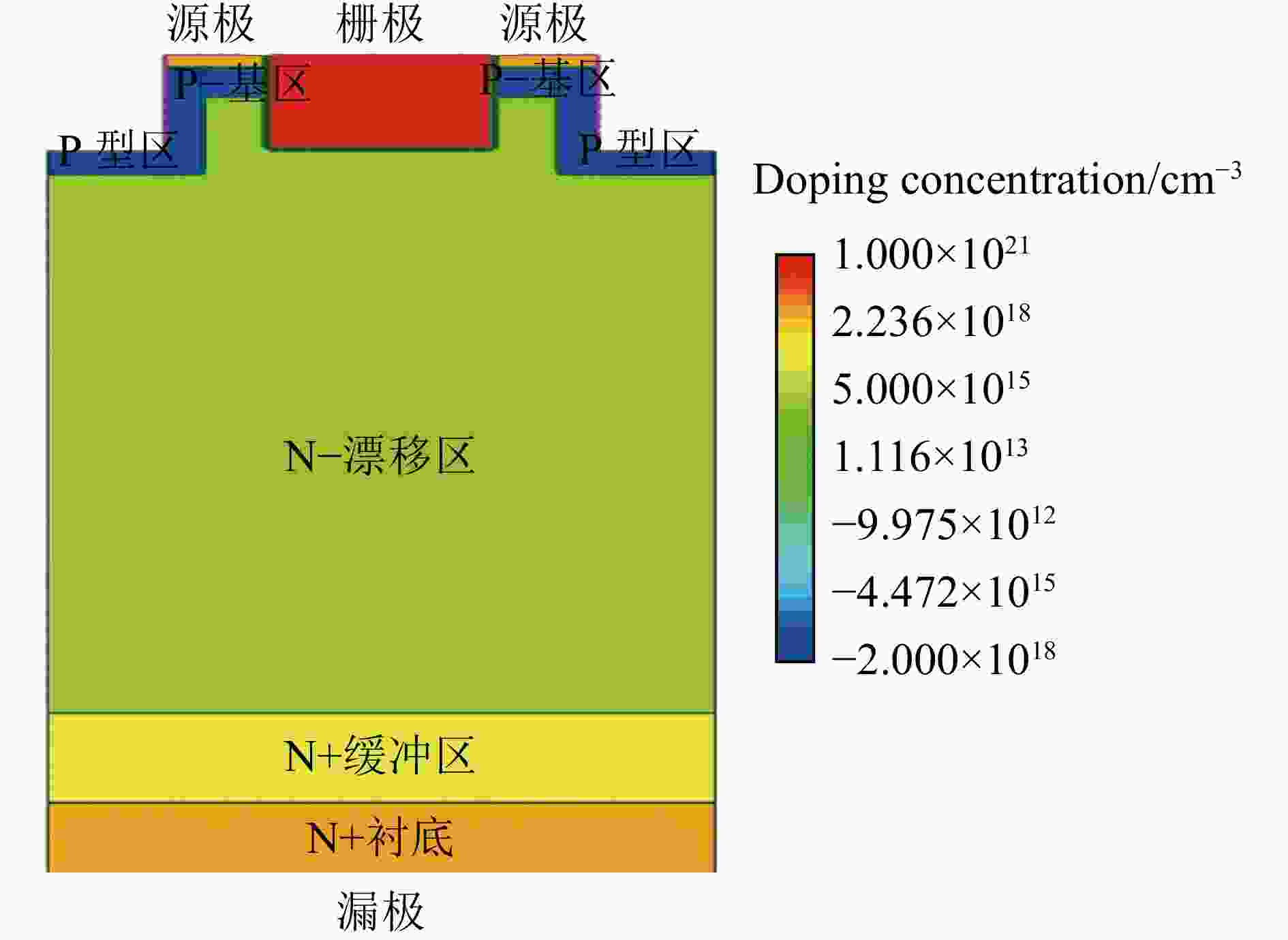
由于SiC双沟槽MOSFET的结构呈轴对称性,本工作选择了该器件的半个单元结构进行单粒子烧毁效应的仿真研究,并对SiC双沟槽MOSFET器件的模拟模型进行网格化处理。仿真选取的重离子入射位置如图3所示,此处靠近器件内部寄生晶体管的所在位置,产生的电子空穴对更易造成寄生晶体管导通,更容易诱发单粒子烧毁效应[8]。由于SiC的熔点一般在2 900至3 100 K范围内[9],本工作设定SiC双沟槽MOSFET器件发生单粒子烧毁效应的临界温度为3 000 K。
-
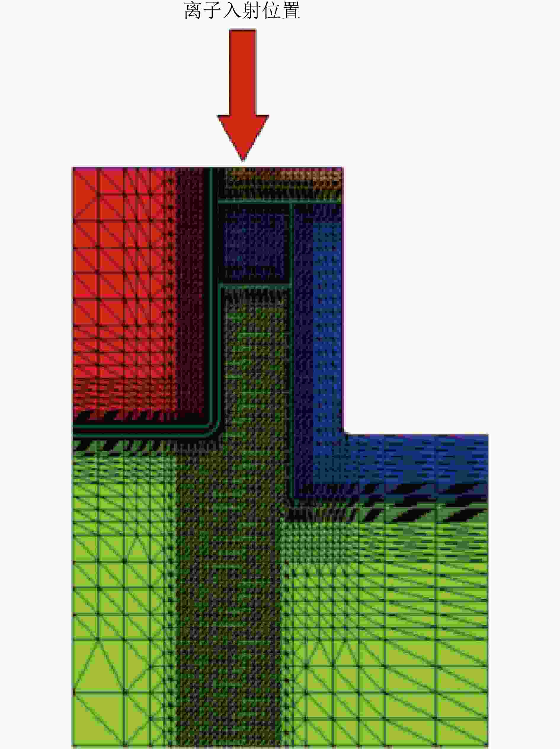
图4(a)给出了当栅源电压为0 V时,漏极电流随时间的变化关系,对应的漏源电压分别为300, 400, 500, 596, 597 V。当重离子垂直入射SiC双沟槽MOSFET器件时,电离产生的电子-空穴对会形成瞬态脉冲电流,并引起漏极电流迅速上升,但若漏源电压较低,漏极电流将会逐渐降低,多余的载流子也会在漏源电压的作用下被逐渐抽出,使器件免于单粒子烧毁效应。而对应本文的模拟器件,如图4(a)所示,当漏源电压为597 V时,器件内部的漏极电流急剧升高,发生单粒子烧毁现象。漏源电压597 V对应于该器件发生单粒子烧毁效应的阈值电压。
不同漏源电压下SiC双沟槽MOSFET器件内部晶格最大温度分布如图4(b)所示。随着漏源电压的不断增大,SiC双沟槽MOSFET器件内部晶格最大温度逐渐升高。当漏源电压为300 V时,晶格最大温度为355.635 K;当漏源电压为400 V时,晶格最大温度为377.33 K;当漏源电压为500 V时,晶格最大温度为596.665 K;当漏源电压为596 V时,晶格最大温度为1 648.206 K。当漏源电压达到单粒子烧毁效应的阈值电压597 V时,此时漏极电流激增,晶格温度急剧升高并达到SiC材料的熔点(3 000 K),单粒子烧毁现象发生。
-
图5(a)给出了漏源电压为597 V时,空穴电流密度在SiC双沟槽MOSFET器件内部的分布情况,Time=1 ps到 Time=1 ns。当高能离子入射SiC双沟槽MOSFET器件时,其电离产生的电子-空穴对会沿着重离子径迹长度方向形成一个等离子体柱,该等离子体柱逐渐扩散,形成瞬态的电流源,由该电流源产生的电荷在漏源电压的作用下移动;此时空穴在漏源电压的作用下通过P基区域向上流向源极,同时产生的空穴也会侧向流入P+区,因此侧向空穴电流增加,使得寄生晶体管的基极和发射极间产生电压,寄生晶体管正向导通。与此同时,电子电流密度在SiC双沟槽MOSFET器件内部的分布情况,如图5(b)所示,Time=1 ps到Time=1 ns。在漏源电压的作用下,电子向下流入N缓冲区和漏极,以维持此处的雪崩效应,同样,寄生晶体管也由雪崩过程产生的空穴电流持续馈电;以上条件最终会导致寄生晶体管的正反馈机制被建立,使得器件内部电流密度增加。从图5(c)不难看出,当Time=1 ns时刻,器件内最大电子、空穴电流密度均远大于其他时刻的最大电子、空穴电流密度。由模拟可以得到,寄生晶体管的正反馈机制会驱动载流子雪崩,导致漏极电流失控,最终引发单粒子烧毁。

-
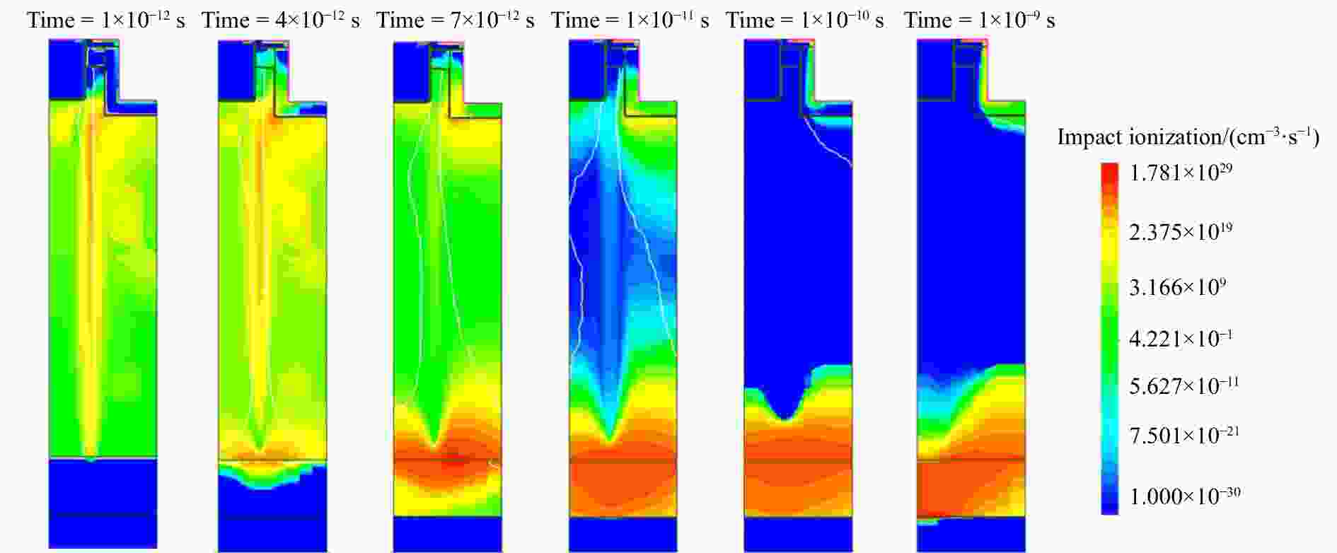
重离子垂直入射SiC双沟槽MOSFET器件,碰撞电离的空间分布如图6所示。碰撞电离主要分布在离子径迹周围以及P型区/N漂移区结处,当寄生晶体管被开启,由于Kirk效应[2]的作用,导致高强度的碰撞电离逐渐由P型区/N漂移区结移动至N漂移区/N缓冲区结处。由于高漏源电压的作用,该区域的雪崩效应会持续存在,产生的空穴电流将会持续为寄生晶体管馈电。特别地,随着该区域的局部电场强度的增强越来越剧烈,晶格温度升高达到临界温度(3 000 K),最终导致器件发生单粒子烧毁效应。
-
图7给出了发生单粒子烧毁效应时,晶格温度、电场强度、碰撞电离在器件内部的空间分布,所选取的时间范围为Time=0.6 ns到Time=1.136 9 ns。这是由于Time=0.6 ns为漏极电流和器件内部最大晶格温度变化趋势的拐点。Time=1.136 9 ns是器件内部SiC材料晶格温度达到3 000 K的临界时刻。由图可以看出,温度峰值首先出现在N漂移区/N缓冲区结处。在Time=0.6 ns到Time=1.136 9 ns时间范围内,该区域的晶格温度大幅升高,最终达到SiC材料晶格熔化的临界温度。在该时间范围内,漏极电流也开始出现不可控的上升趋势,与晶格温度有着相同的变化趋势。同时对比该时间段,N漂移区/N缓冲区结处的碰撞电离强度和电场强度相较于器件内其他区域,也一直处于较高水平。由于漏源电压达到了单粒子烧毁的阈值电压(597 V),寄生晶体管导通,产生Kirk效应,寄生晶体管基区展宽至N漂移区/N缓冲区结处,此处的强电场诱发高强度碰撞电离,产生大量的电子空穴对,进一步促进了自热效应,导致器件内部温度持续升高。

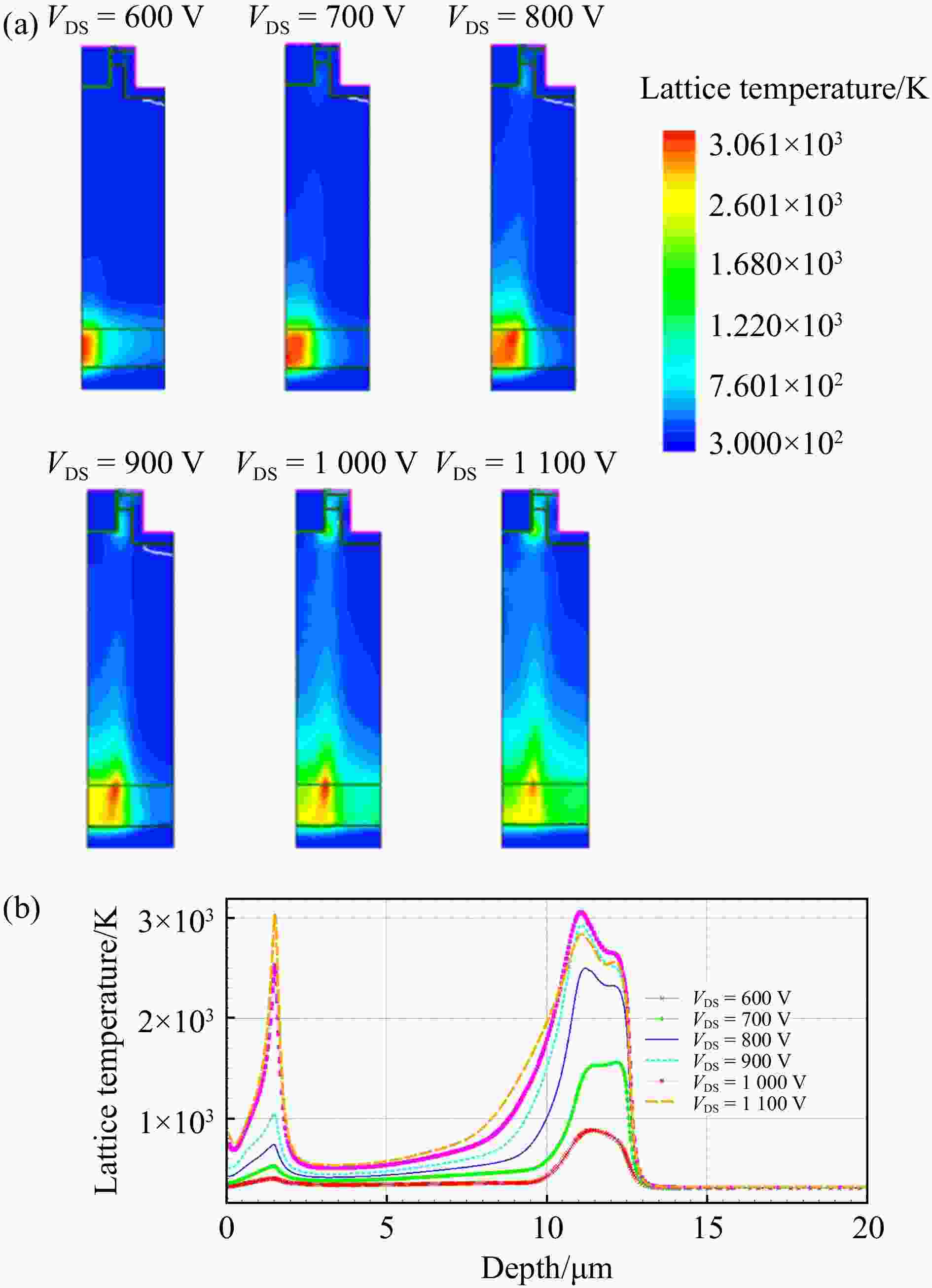
在模拟单粒子烧毁效应时,对比了不同漏源电压下晶格温度在器件内部的分布情况,如图8(a)、(b)所示。当漏源电压由600增加至800 V时,N漂移区/N缓冲区结处首先达到临界温度,且随漏源电压的增大,高温区域在N缓冲区内扩展;而当漏源电压逐渐增加至900,1 000 V时,沟槽栅与N漂移区结处温度开始逐渐升高;当漏源电压为1 100 V时,沟槽栅与N漂移区结处首先达到临界温度,随后在N漂移区/N缓冲区结处观察到第二个温度峰值,温度峰值靠近位于离子入射径迹附近。
-
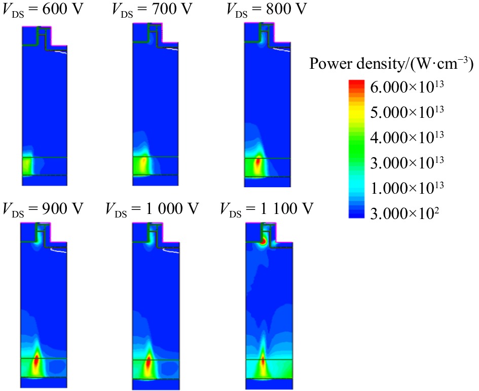
器件的功率密度定义为电流密度乘以电场强度[3],用于反映SiC MOSFET局域内的功率耗散。局部区域功率耗散过大会导致SiC材料晶格熔化[3]。针对器件内部达到临界温度状态,TCAD程序模拟计算了不同源漏偏置电压下的器件内部功率密度空间分布如图9所示。功率密度的峰值区域与晶格温度的峰值区域对应一致,这是由于在器件内局部发生的雪崩效应会导致强电场的产生,造成了过大的功率耗散。当漏源电压为600, 700, 800, 900 V时,在N漂移区/N缓冲区结处观察到明显的功率密度。而随着漏源电压增加至1 000, 1 100 V时,在沟槽栅与N漂移区结处出现第一个功率密度峰值,随后在N漂移区/N缓冲区结处出现第二个功率密度峰值,该现象与晶格温度的变化趋势相同。
-
本工作采用TCAD程序开展重离子入射条件下SiC双沟槽MOSFET器件的单粒子烧毁效应模拟仿真研究,建立了SiC双沟槽MOSFET器件的单粒子烧毁效应模拟模型,模拟计算了当SiC双沟槽MOSFET器件发生单粒子烧毁效应时,器件内部电子电流密度、空穴电流密度、电场强度、晶格温度、碰撞电离等物理量的空间分布,以此分析得出器件内发生单粒子烧毁效应的主要成因——器件内寄生双极晶体管导通及正反馈机制被建立,由于漏源电压达到了单粒子烧毁的阈值电压(597 V),此时寄生晶体管导通,Kirk效应增强,基区展宽至N缓冲区强电场诱发高强度碰撞电离,产生大量的电子空穴对,进一步促进了自热效应,导致器件内部温度持续升高,晶格温度峰首先出现在N漂移区/N缓冲区结处。同时评价给出了漏源电压对关态器件下的单粒子烧毁效应的影响,当漏源电压由600增加至800 V时,N漂移区/N缓冲区结处首先达到临界温度,且随漏源电压的增大,高温区域在N缓冲区内扩展;而当漏源电压逐渐增加至900, 1 000 V时,沟槽栅与N漂移区结处温度开始逐渐升高;当漏源电压为1 100 V时,沟槽栅与N漂移区结处首先达到临界温度,随后在N漂移区/N缓冲区结处观察到第二个晶格温度峰;同时分析了器件内部功率密度与晶格温度关系,随着漏源电压的增加,功率密度峰出现位置对应晶格温度峰的产生位置;为SiC双沟槽MOSFET器件的抗核加固技术提供了结构方案和数据支持。
Simulation Study on Single-Event Burnout Effect in SiC DT-MOSFET
doi: 10.11804/NuclPhysRev.40.2022106
- Received Date: 2022-10-13
- Rev Recd Date: 2022-12-05
- Publish Date: 2023-09-20
-
Key words:
- SiC DT-MOSFET /
- single event effect /
- single event burnout /
- lattice temperature
Abstract: SiC DT-MOSFET are prone to single event burnout(SEB) effect under heavy ion incident conditions. In this work, the TCAD program is used to simulate and calculate the spatial distribution of physical quantities such as drain curren, current densityt, lattice temperature, collision ionization and power density inside the device, and evaluate the influence of bias voltage on SEB effect. According to the simulation results, the transient current source formed by the incident ions turns on the parasitic bipolar transistor, the high drain source voltage maintains the avalanche effect in the device, and then the positive feedback mechanism of the device is established. Finally, the generated transient high current leads to the thermal damage of the device. Therefore, the main cause of SEB effect in SiC DT-MOSFET is the conduction of parasitic bipolar transistor and the establishment of positive feedback mechanism. In addition, the effect of strong electric field on collision ionization, lattice temperature and power density distribution is evaluated, and the reason why the peak region of power density corresponds to the peak region of lattice temperature is revealed, which provides data support for the anti nuclear reinforcement technology of SiC DT-MOSFET.
| Citation: | Jinqiu PENG, Hang ZHANG, Kang WU, Xingyu LIU, Xu YANG, Xiaohou BAI, Zheng WEI, Zeen YAO, Junrun WANG, Tianzhi JIANG, Chao BAO, Jiawei LU, Yu ZHANG. Simulation Study on Single-Event Burnout Effect in SiC DT-MOSFET[J]. Nuclear Physics Review, 2023, 40(3): 459-465. doi: 10.11804/NuclPhysRev.40.2022106

|


 甘公网安备 62010202000723号
 DownLoad:


