


-
宇宙空间中由于没有大气层和地磁场的保护,存在着大量高能粒子,高能粒子射线会造成卫星等飞行器内部的微电子器件电学性能出现改变或者退化,并最终导致微电子器件功能异常甚至失效[1-4],因此,宇航设备中的微电子器件有着较高的抗辐射可靠性需求。
与传统体硅器件相比,FDSOI器件由于埋氧层实现了全介质隔离,消除了体硅CMOS电路中的锁定效应,增强了栅极对沟道的控制作用,并使器件具有速度快、功耗低等优势[5-8]。SOI CMOS工艺比体硅CMOS工艺具有更为优异的抗瞬态剂量率[9-10]和抗SEU[11]能力,因此其在先进商业器件中的应用比例日渐提升,也是下一代军用系统集成的主要技术之一。研究表明[12-14],FDSOI工艺SRAM存储阵列自身的抗SEU能力很强,在抗MCU方面也有着非常出色的表现。当对FDSOI SRAM存储阵列采取一定的加固措施后,即使在重离子大角度入射下,也可以很好地抑制MCU。随着现代微电子技术的发展,器件栅长特征尺寸的持续减小,导致相邻敏感节点间距缩短以及SEU临界电荷降低,MCU在SOI工艺器件SEU中的占比提升对器件的单粒子可靠性提出新的要求[15-20]。在国内外,提高SRAM等电路抗SEU能力的重要途径之一就是采用加固的FDSOI CMOS工艺进行制造,FDSOI器件已经成为了当前技术环境的最优选择之一。
但是随着器件工艺尺寸的缩小、工作频率的提高,影响先进纳米工艺SRAM器件MCU的物理机制尚不完全清晰,尤其对于先进纳米节点FDSOI工艺集成电路的重离子单粒子效应研究较少[21]。实验研究先进纳米器件的MCU规律,并分析其背后的物理机制对全面提高FDSOI工艺SRAM的抗MCU能力非常重要。因此,我们将对工艺节点为22 nm的FDSOI SRAM器件SEU截面和MCU比例进行实验研究,揭示不同LET、入射角度和工作电压对FDSOI器件SEU截面和MCU比例的影响规律。
-
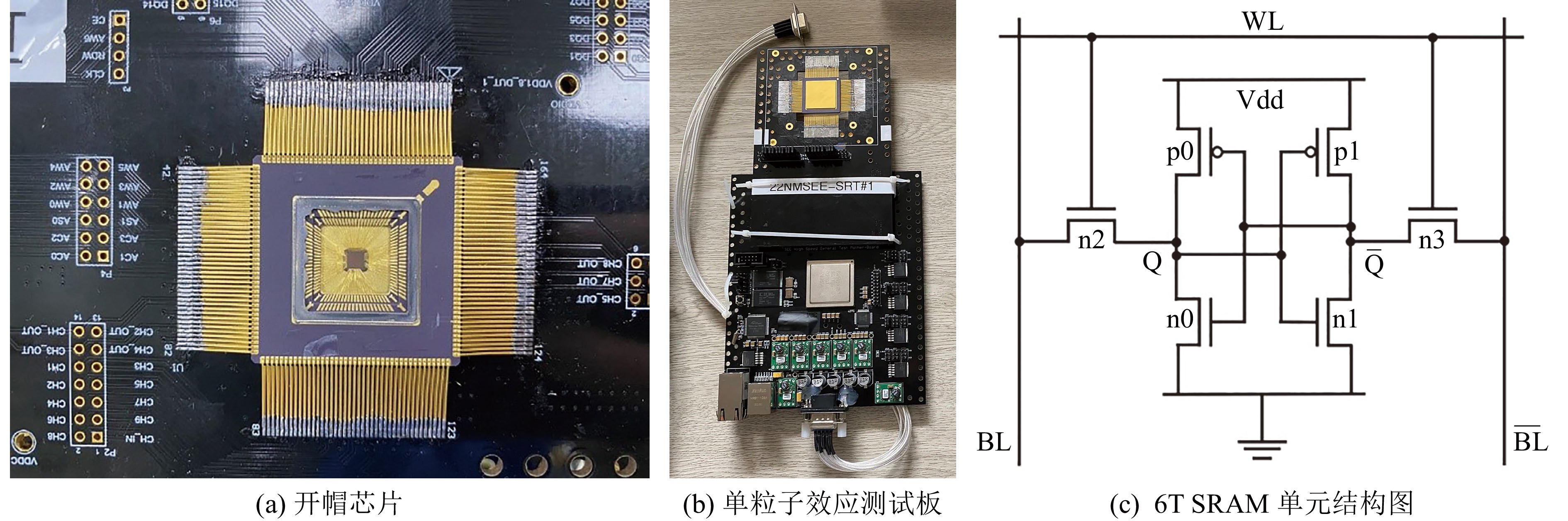
重离子辐照实验所用的器件为22 nm全耗尽型绝缘体上硅(Fully Depleted Silicon on Insulator, FDSOI)的测试片。芯片和测试板如图1所示,实验被测芯片为22 nm FDSOI工艺的6T SRAM。SRAM器件的存储容量为128 K,具有13个地址位和16个数据位。图1(a)所示为辐照实验前已开帽的SRAM器件,开帽可以保证入射离子能够到达灵敏区。实验前对器件进行了功能测试,以确保待测芯片能够在标准电压以及高低拉偏电压下正常工作。

图 1 22 nm FDSOI 6T SRAM(在线彩图)
-
本工作基于中国科学院近代物理研究所HIRFL加速器和北京原子能研究院HI-13串列加速器单粒子效应实验终端,利用不同种类重离子对该款器件进行了单粒子效应实验,实验条件及参数如表1所列。如图2所示, DUT(Device under Test)在HIRFL的TR5单粒子效应测试终端的大气辐照平台进行辐照测试。原子能研究院HI-13串列加速器辐照实验时,DUT被放置于真空罐中进行辐照测试。测试系统每次辐照前都要进行复位和写入数据图形,开始读操作后测试系统不断地循环读取存储阵列的数据并与预设数据图形比对,当发现错误事件后,系统会自动记录相应的错误地址和数据等信息。实验中实时观察器件工作电流,若达到限流,立即断电并记录该实验条件。
表 1 SRAM实验条件及参数
实验条件 实验参数 角度/(°) α = 0,90;β = 0,30,60 核心电压/V 0.54,0.72,0.80,0.90,1.08,1.26 LET/(MeV·cm2·mg−1) 8.7,13.4,22.2,37.4,75.4,78.1 
图 2 Ta离子辐照单粒子效应测试实验(在线彩图)
在HIRFL加速器开展辐照实验时,我们利用能量为16 MeV/u的181Ta离子开展重离子辐照实验,研究被测器件饱和区的SEU敏感性。我们使用SRIM-2013详细地计算了重离子参数,确定获得每个能量条件所需的铝箔降能片和空气层厚度,通过调整被测器件和离子束流出窗口之间的铝箔降能片和空气层厚度以获得能量较低、LET较大的实验条件。原子能研究院HI-13加速器开展辐照实验时,我们选用了四种LET较低的重离子进行实验,实验中通过改变重离子类型来改变LET。
辐照前先让测试系统进入正常工作状态,辐照开始后翻转数达到400个或重离子总注量达到1×10⁷ ions/cm2时,停止辐照并记录数据,以保证实验数据具有统计意义。
-
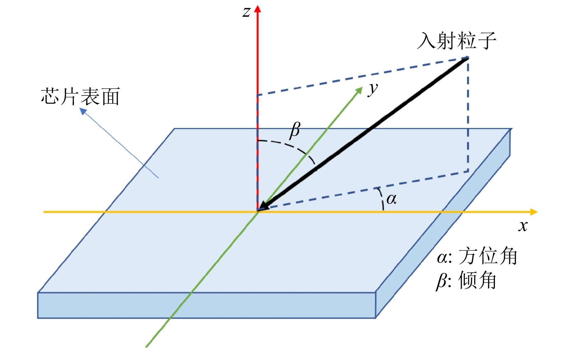
如表2所列,我们在HIRFL和HI-13进行了不同LET的重离子辐照实验,重离子射程范围从30到116.6 μm,所有离子射程都能到达器件的灵敏区。除了空气层厚度为70 mm的Ta离子实验进行了入射角度的改变,其余实验均使重离子沿器件表面的法线方向入射。在I/O电压1.62 V、核心电压0.72 V条件下研究LET较低时器件SEU截面和MCU比例随重离子LET增加的变化趋势,在I/O电压1.8 V、核心电压0.9 V条件下研究高LET下器件的SEU截面和MCU比例随入射角度改变的变化趋势。如图3所示,当离子入射方位角α分别为0°和90°,离子将沿芯片的两个互相垂直的方向入射,研究离子入射方位角对器件SEU敏感性的影响;随后,改变这两个方向下离子入射倾角β的大小,研究离子入射方向和芯片表面法线所成角度对SEU敏感性的影响。
表 2 重离子辐照实验参数
离子
种类空气
厚度/mm铝箔
厚度/μm能量/MeV LET/
(MeV·cm2·mg-1)Si中
射程/μmTa 40 0 2 006.4 75.4 116.6 70 0 1 721.4 78.1 100.7 Al 0 0 110.0 8.7 48.0 Cl 0 0 150.0 13.4 42.8 Ti 0 0 160.0 22.2 32.9 Ge 0 0 205.0 37.4 30.0 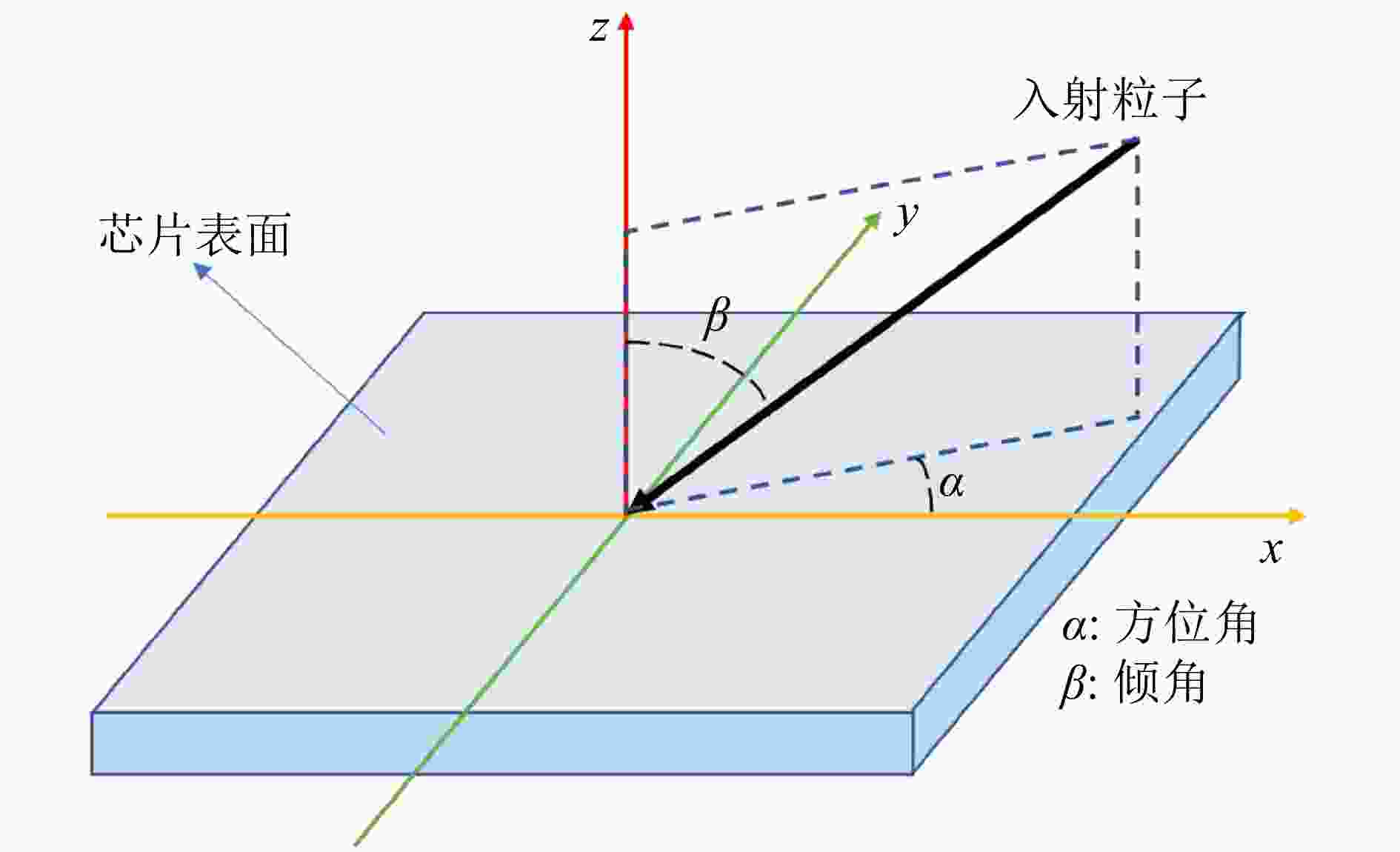
图 3 辐照角度示意图(在线彩图)
-
单粒子测试系统记录了出现SEU的逻辑地址和错误数据,我们根据在同一时间范围内的翻转数量和逻辑位图,对不同翻转位数的MCU的数量进行了统计分析和研究。计算并研究了比特截面(SEU bit cross section)、事件截面(SEU event cross section)以及MCU比例。计算方式如下。
比特截面:
$$ \begin{split} {\sigma }_{\mathrm{U}-\mathrm{S}\mathrm{E}\mathrm{U}}=& \sum _{i=1}^{\mathrm{\infty }}\frac{i\times {E}_{i-\mathrm{b}\mathrm{i}\mathrm{t}}}{\varPhi \times \mathrm{c}\mathrm{o}\mathrm{s}\beta } \\ =&\frac{{1\times E}_{1-\mathrm{b}\mathrm{i}\mathrm{t}}+{2\times E}_{2-\mathrm{b}\mathrm{i}\mathrm{t}}+{3\times E}_{3-\mathrm{b}\mathrm{i}\mathrm{t}}+\dots }{\varPhi \times \mathrm{c}\mathrm{o}\mathrm{s}\beta }, \end{split}$$ (1) 事件截面:
$$ \begin{split} {\sigma }_{\mathrm{E}-\mathrm{S}\mathrm{E}\mathrm{U}}=& \sum _{i=1}^{\mathrm{\infty }}\frac{{E}_{i-bit}}{\varPhi \times \mathrm{c}\mathrm{o}\mathrm{s}\beta } \\ =&\frac{{E}_{1-\mathrm{b}\mathrm{i}\mathrm{t}}+{E}_{2-\mathrm{b}\mathrm{i}\mathrm{t}}+{E}_{3-\mathrm{b}\mathrm{i}\mathrm{t}}+{E}_{4-\mathrm{b}\mathrm{i}\mathrm{t}}+\dots }{\varPhi \times \mathrm{c}\mathrm{o}\mathrm{s}\beta }, \end{split} $$ (2) 其中:i是一个SEU事件中受到影响的单元数;
$ {E}_{i-\mathrm{b}\mathrm{i}\mathrm{t}} $ 是一个事件中的翻转单元数;Ф是重离子注量和器件存储容量的乘积,如图3所示入射倾角β是重离子入射方向与芯片表面法线的夹角。计算MCU比例的公式如下所示:$$ {P}_{n-\mathrm{b}\mathrm{i}\mathrm{t}} = \frac{{E}_{n-\mathrm{b}\mathrm{i}\mathrm{t}}}{{E}_{1-\mathrm{b}\mathrm{i}\mathrm{t}}+{E}_{2-\mathrm{b}\mathrm{i}\mathrm{t}}+{E}_{3-\mathrm{b}\mathrm{i}\mathrm{t}}+{E}_{4-\mathrm{b}\mathrm{i}\mathrm{t}}+\dots }, $$ (3) 单粒子事件数据分布通常为高斯(正态)分布;N个事件的标准偏差为N1/2;百分比标准偏差为N1/2/N=1/N1/2。
-
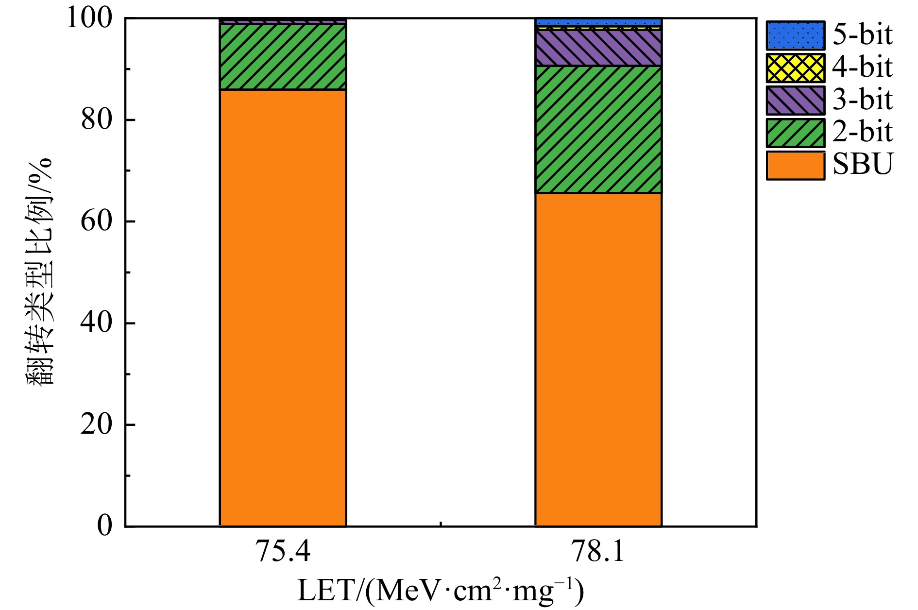
首先是在HIRFL的TR5单粒子效应终端进行的Ta离子实验,实验中设置I/O电压为1.8 V、核心电压为0.9 V。图4为LET为75.4和78.1 MeV·cm2·mg−1的SEU比特截面和事件截面,可以判断器件SEU截面已经达到饱和,因此Ta离子实验处在器件的饱和区。虽然图4中LET从75.4增加到78.1 MeV·cm2·mg−1对截面影响较小,但是从图5可以看出,LET = 78.1 MeV·cm2·mg−1的MCU比例明显高于LET = 75.4 MeV·cm2·mg−1的比例。因此,图4中SEU比特截面增高而事件截面下降是因为在LET为78.1 MeV·cm2·mg−1下的MCU比例要高于LET在75.4 MeV·cm2·mg−1下的MCU比例。该实验结果背后的物理机制是重离子电离径迹会影响到小节点器件的多个单元,LET越大,则电离径迹中心附近的灵敏区收集到更多电荷,所以更容易出现MCU。

图 4 饱和区内SEU截面随LET增加的变化趋势(在线彩图)
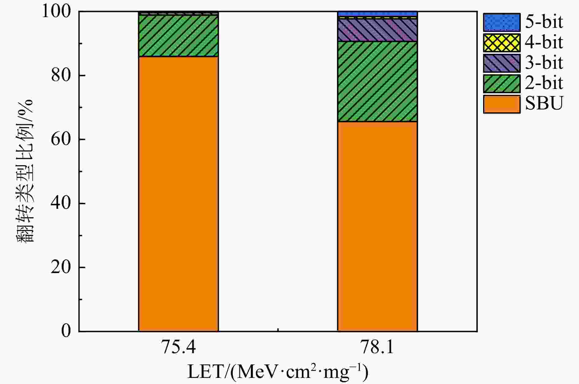
图 5 饱和区内MCU比例随LET增加的变化趋势(在线彩图)
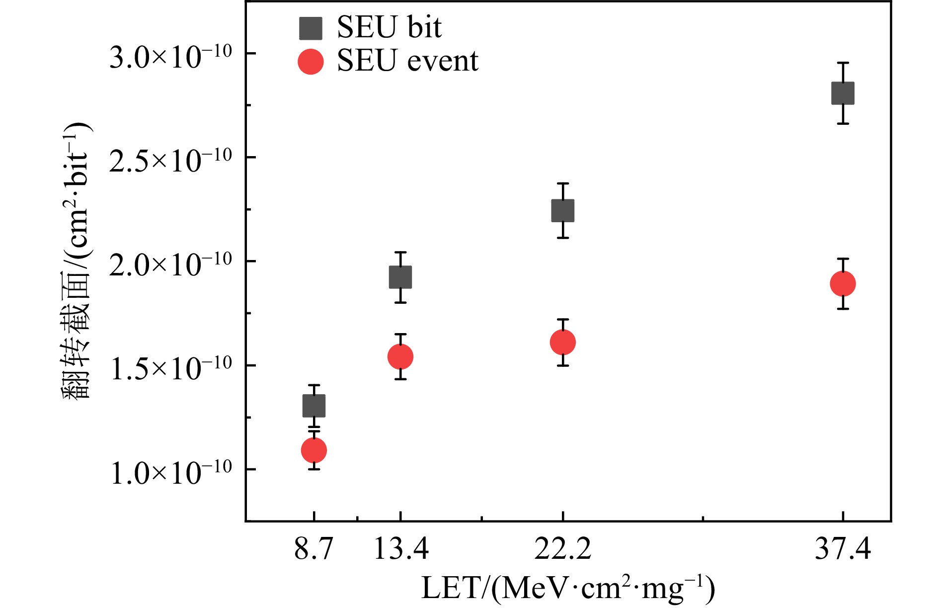
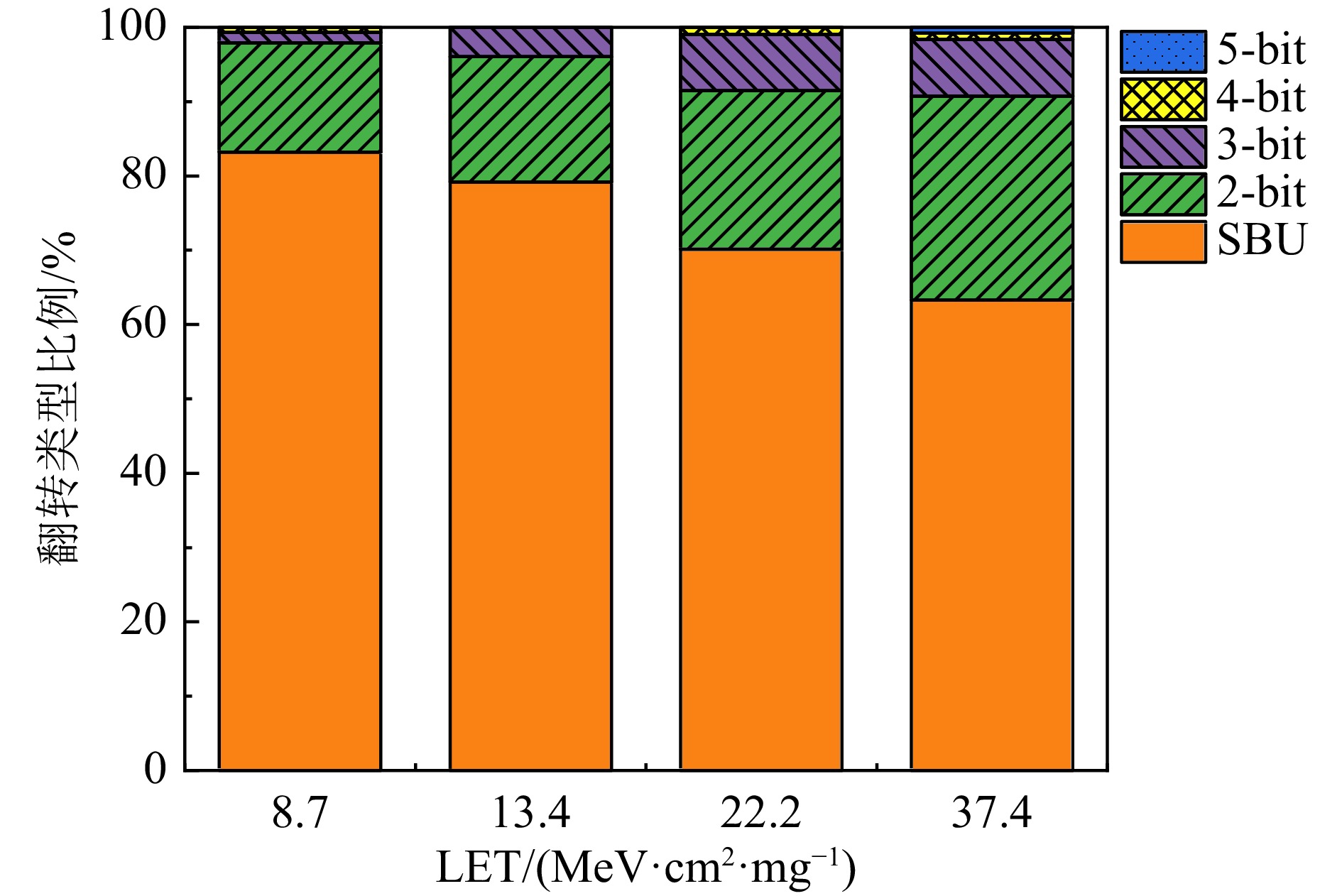
我们在北京原子能研究院进行了低LET值SEU实验研究,低电压偏置条件是器件较为敏感的配置状态,为了更精准的评估器件的在轨可靠性及失效率,特别是LET对MCU比例的影响,在LET较低的实验中对电压进行了低拉偏,I/O电压设置为1.62 V,核心电压设置为0.72 V。如图6所示,当LET从8.7 增加到37.4 MeV·cm2·mg−1时,器件的SEU截面明显增大,这与饱和区的SEU截面趋势不同,在非饱和区,SEU截面随着LET的增大出现了很明显的上升趋势。如图7所示,MCU的比例随着LET的增加而增加。因此,无论在饱和区还是非饱和区,MCU比例对LET都有着很强的依赖性。在图5中LET仅增加2.7 MeV·cm2·mg−1,MCU的比例增加17%;图7中LET从8.7到37.4 MeV·cm2·mg−1增加了28.7 MeV·cm2·mg−1,MCU的比例增加20%;图7中LET增大的部分是图5中增大部分的10倍,而MCU增加的比例相差不大。因此,在高LET下的MCU比例随LET增大的斜率要远大于低LET。其背后的物理机制为,高LET的重离子能量降低(LET改变)后,电离径迹核心高密度区域尺寸变大更明显,进而影响更多的SRAM单元,因此高LET段离子对器件的MCU比例影响更明显。
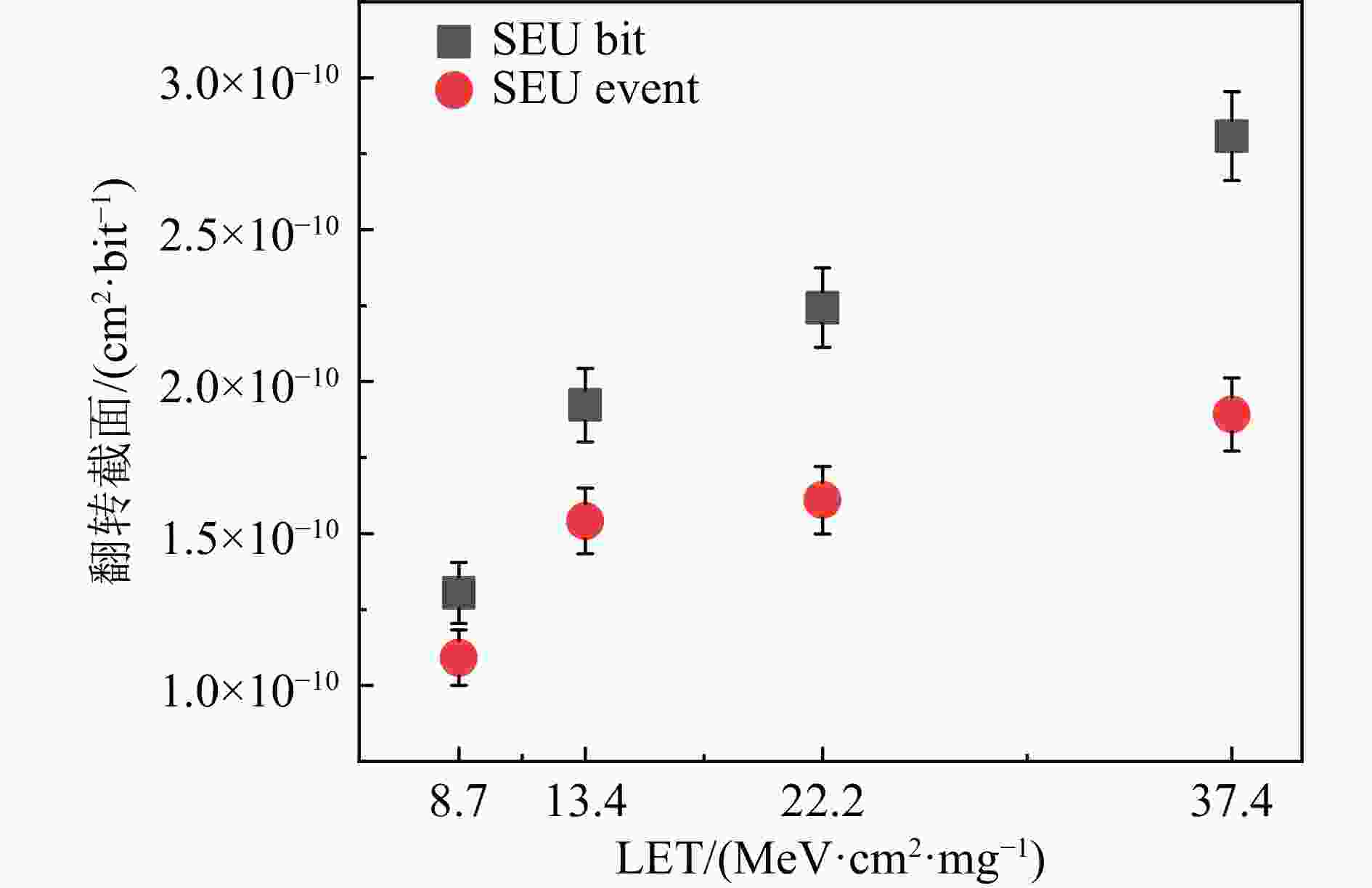
图 6 非饱和区内SEU截面随LET增加的变化趋势(在线彩图)
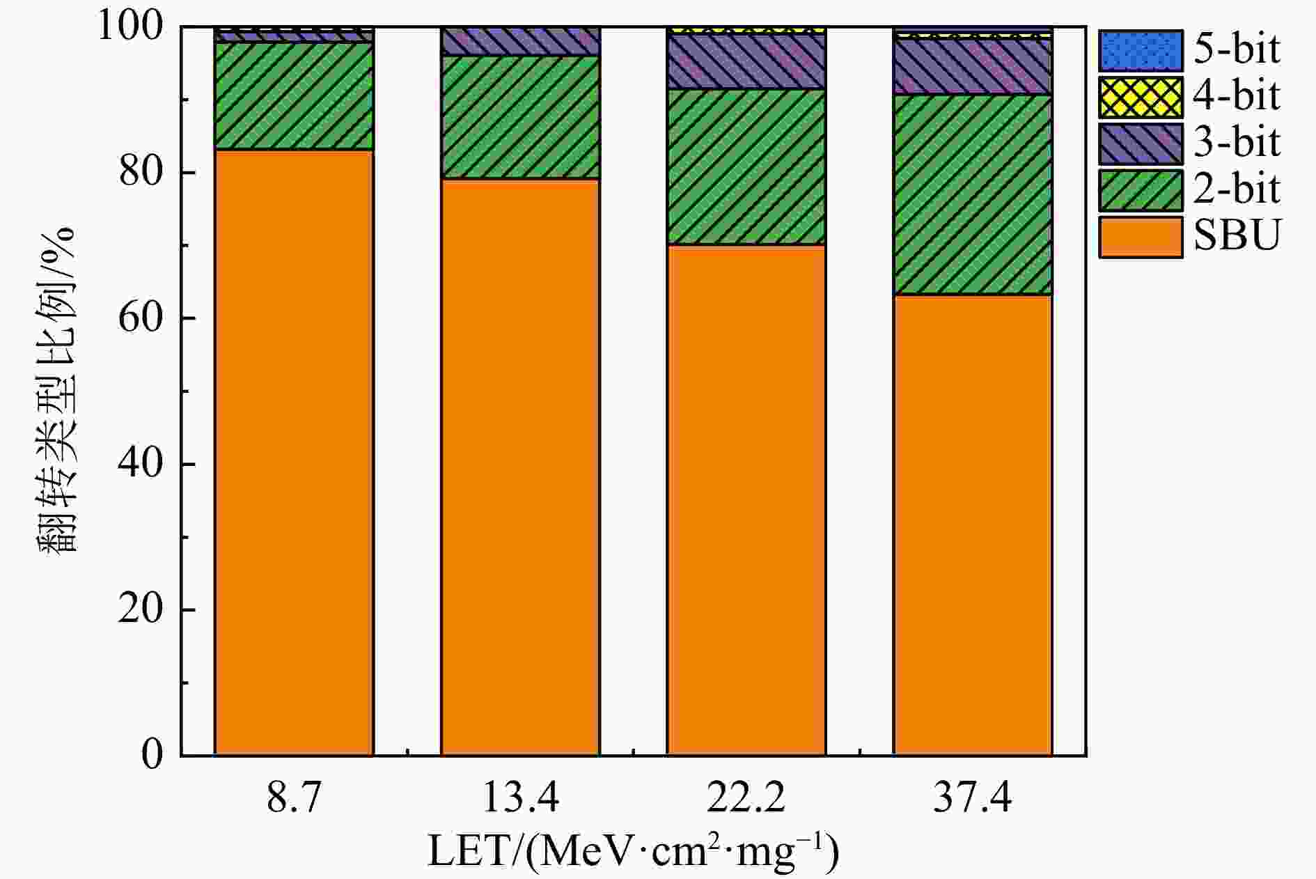
图 7 非饱和区内MCU比例随LET增加的变化趋势(在线彩图)
图8为重离子电离径迹覆盖器件单元的示意图,其中一个黄色的小方块为一个6T SRAM单元。SRAM器件单元面积为0.11 μm²,可得SRAM单元边长约为332 nm。实验中选用的低LET重离子电离半径值约为1 μm,高LET的Ta离子电离半径远超过1 μm [22-26]。图8(a)中为电离半径1 μm的重离子电离径迹覆盖器件单元的示意图,图8(b)为LET增大后的电离径迹中心电荷浓度增大的示意图,LET增大会使靠近重离子径迹中心的电荷浓度增高,使径迹中心附近的SRAM单元灵敏区收集到足够的电荷并发生SEU。因此,增大LET会导致电离径迹影响到更多单元中的灵敏区,进而导致MCU的比例增大。
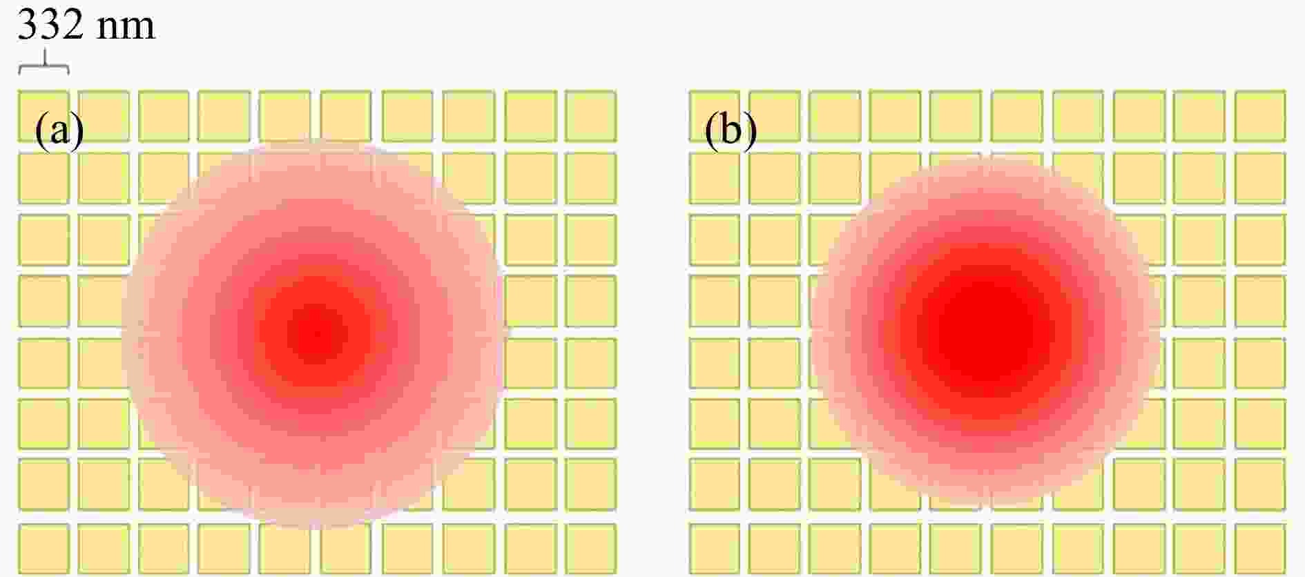
图 8 重离子入射径迹示意图(在线彩图)
-
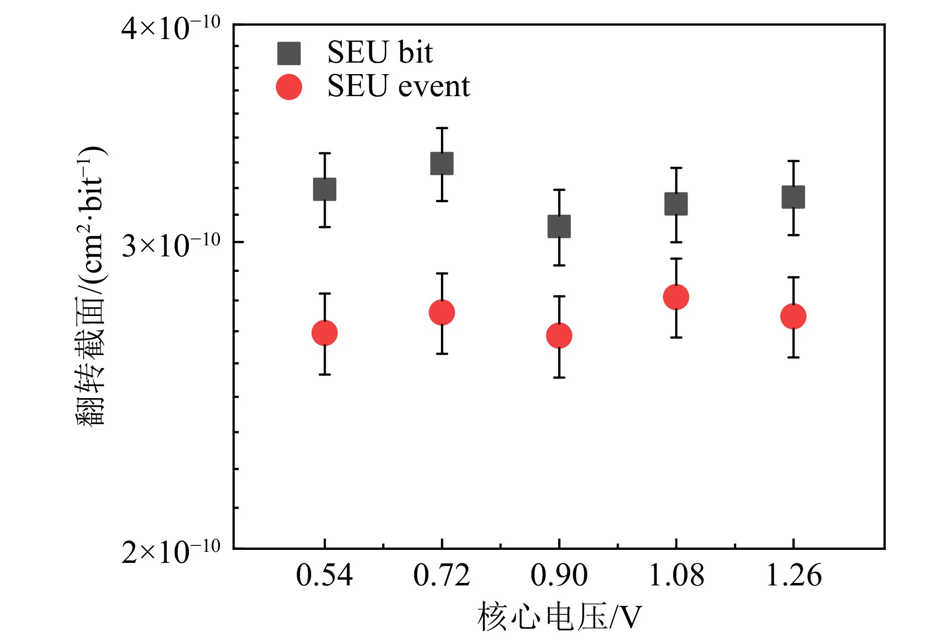
我们利用Ta离子开展了核心电压对器件单粒子敏感性的研究,核心电压的降低一方面会减小器件的驱动电流和SRAM的临界电荷,另一方面也减少了灵敏区收集的电荷。而SEU截面的大小是由临界电荷和收集电荷之间的竞争关系决定的。实验中的I/O电压设置为1.8 V,探究核心电压的改变对单粒子敏感性的影响。通常认为降低电源电压会导致 SRAM 中的SEU临界电荷量减少,从而会加剧 SEU 和MCU的发生[27-30]。而在我们的实验结果中,如图9所示,在LET为75.4 MeV·cm2·mg−1的Ta离子入射的情况下,SEU截面会随着电源电压的变化而波动,但无明显趋势,这表明在被测SRAM的临界电荷和收集电荷的竞争中,没有一方占据主导地位。
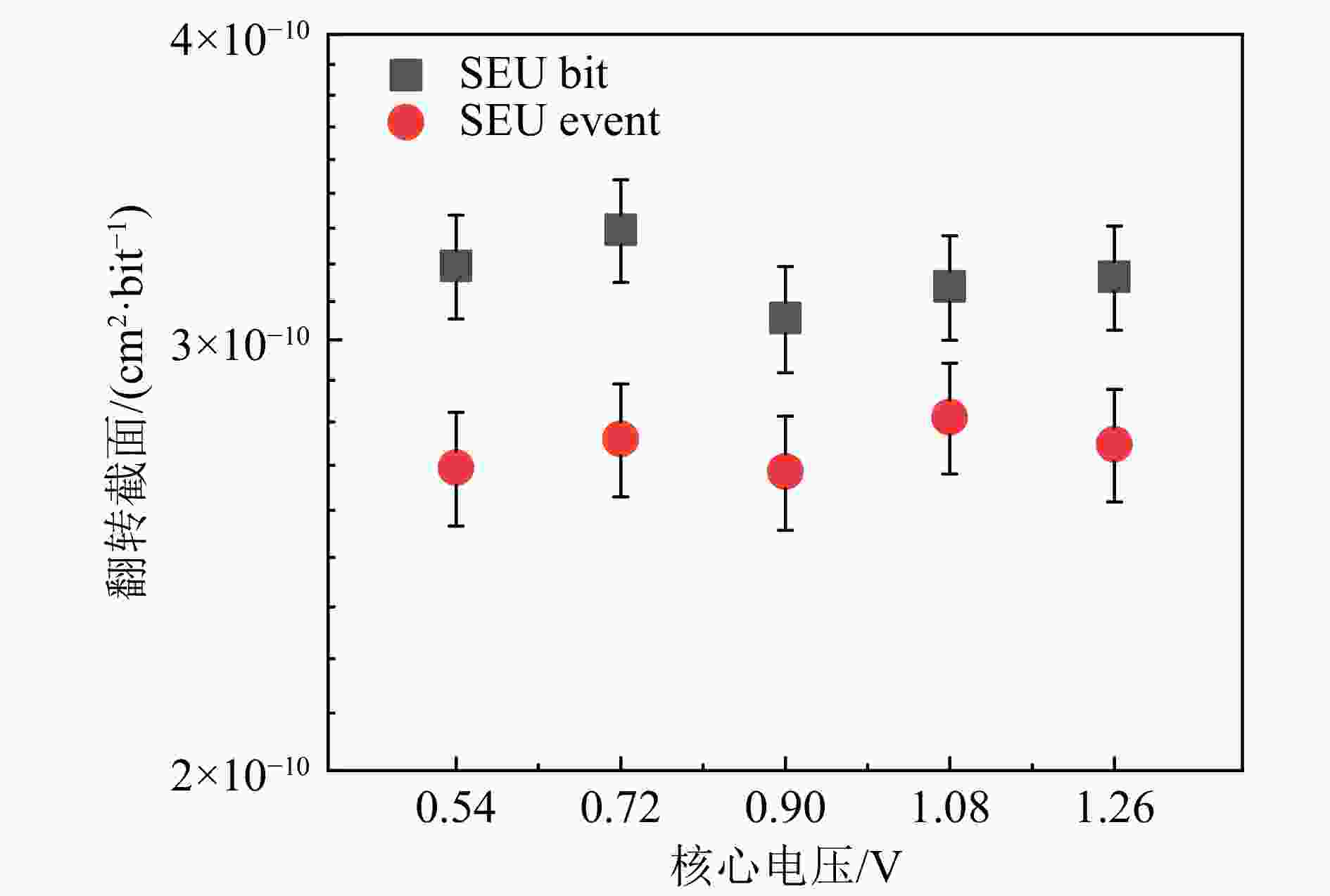
图 9 饱和区内SEU截面随核心电压的变化趋势(在线彩图)
我们统计了每个电压下的MCU比例,结果如图10所示,MCU的比例随着电压变化也无明显趋势,这说明对于这款22 nm FDSOI SRAM而言,在饱和区内,核心电压对器件的SEU比特截面、事件截面以及MCU比例基本没有影响,这是因为实验所选用的LET远超所选取的每个核心电压下的SEU阈值。
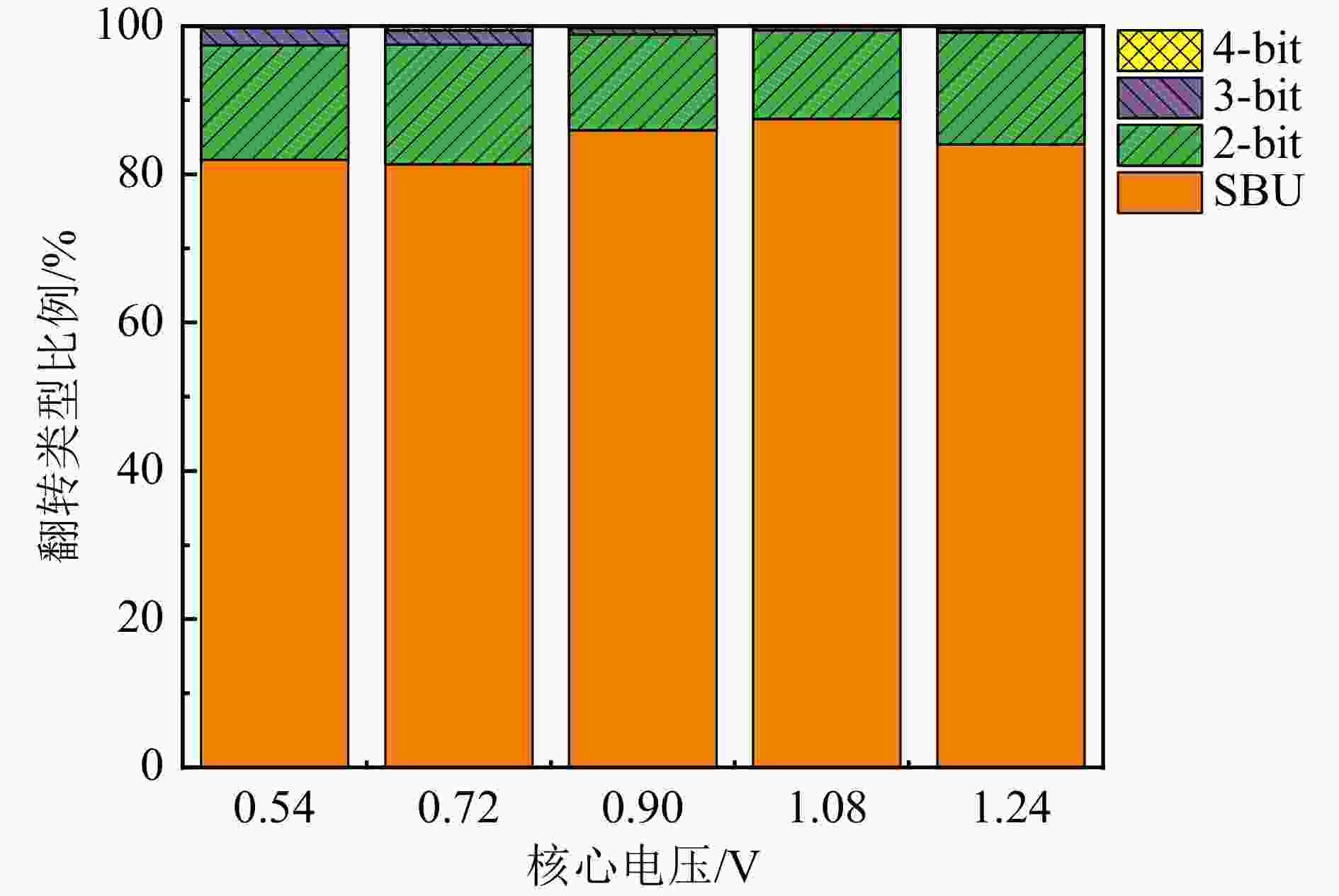
图 10 饱和区内MCU比例随核心电压的变化趋势(在线彩图)
-
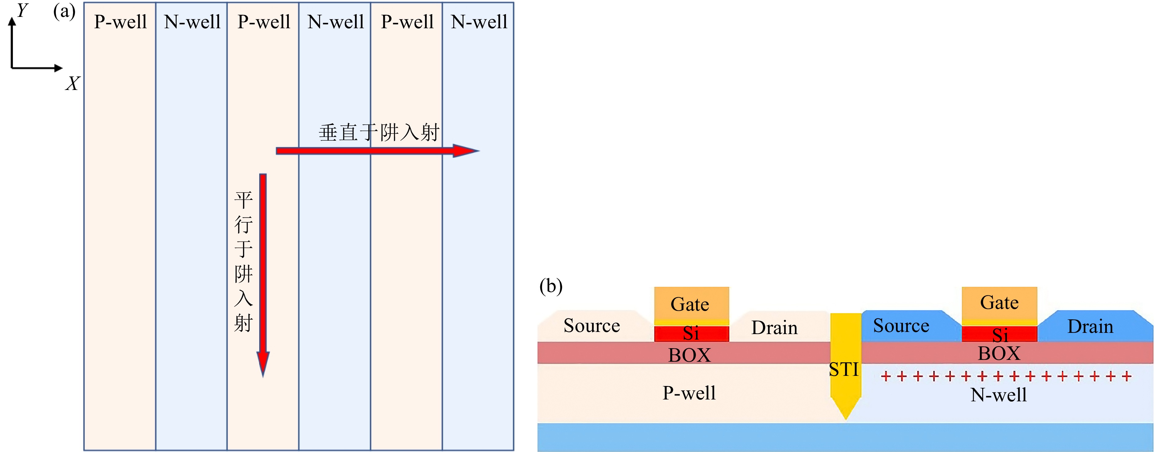
图11为SRAM的SEU截面随重离子沿不同方位角、不同倾角入射的变化趋势,重离子沿待测芯片Y方向(α = 90°)入射时,比特截面有着很明显的变化,而沿X方向(α = 0°)入射时比特截面变化不大;当沿Y方向60°入射时,比特截面增大了2.5倍,比特截面对重离子沿Y轴入射的依赖性更强。对于事件截面,也有同样的差异性,Y方向比X方向更敏感。SEU比特截面和事件截面都对Y方向入射有更强的依赖性,因为Y方向与阱平行,当重离子沿平行阱方向入射时,BOX下方的阱区中的电荷会沿阱运动,其中电子的运动速度大于空穴的速度,空穴暂时滞留在源漏体底部的阱区,产生一个由阱区指向源漏体的电场,拉低源体结和漏体结的势垒高度,进而增大了SEU敏感性。而沿垂直阱方向入射时,如图12所示,P阱和N阱之间有浅槽隔离(Shallow Trench Isolation, STI)阻隔电荷的传输,源漏体底部的阱区产生的电场更弱,因此垂直于阱入射对SEU增幅影响较小。此外,从图11中可以看出,无论平行于阱(α = 90°)入射还是垂直于阱(α = 0°)入射,在β = 60°的大倾角下,SEU截面的增加比β = 30°时更加明显。因此,重离子大角度入射实验对器件抗辐射性能的评估非常有必要。
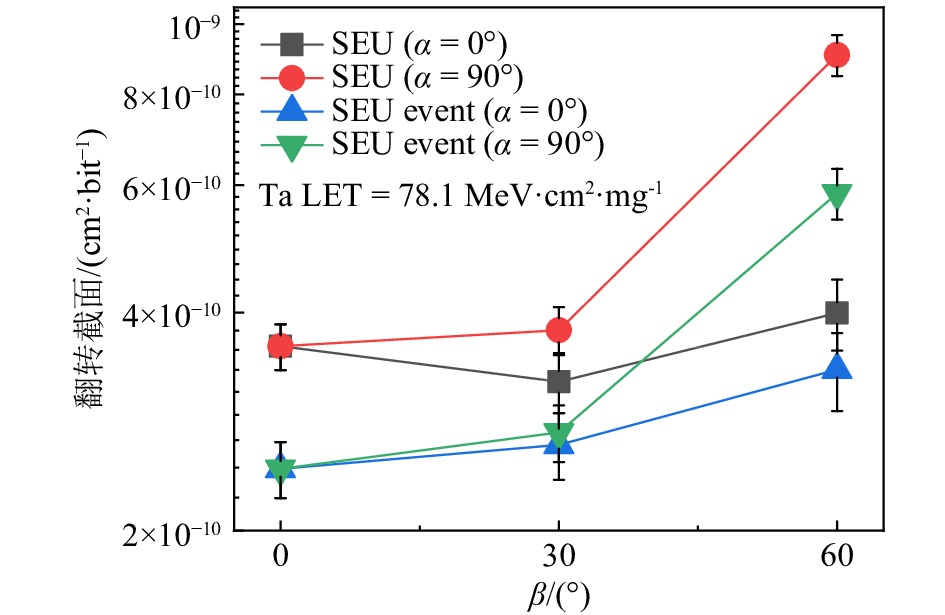
图 11 SEU截面随重离子入射角度的变化趋势(在线彩图)
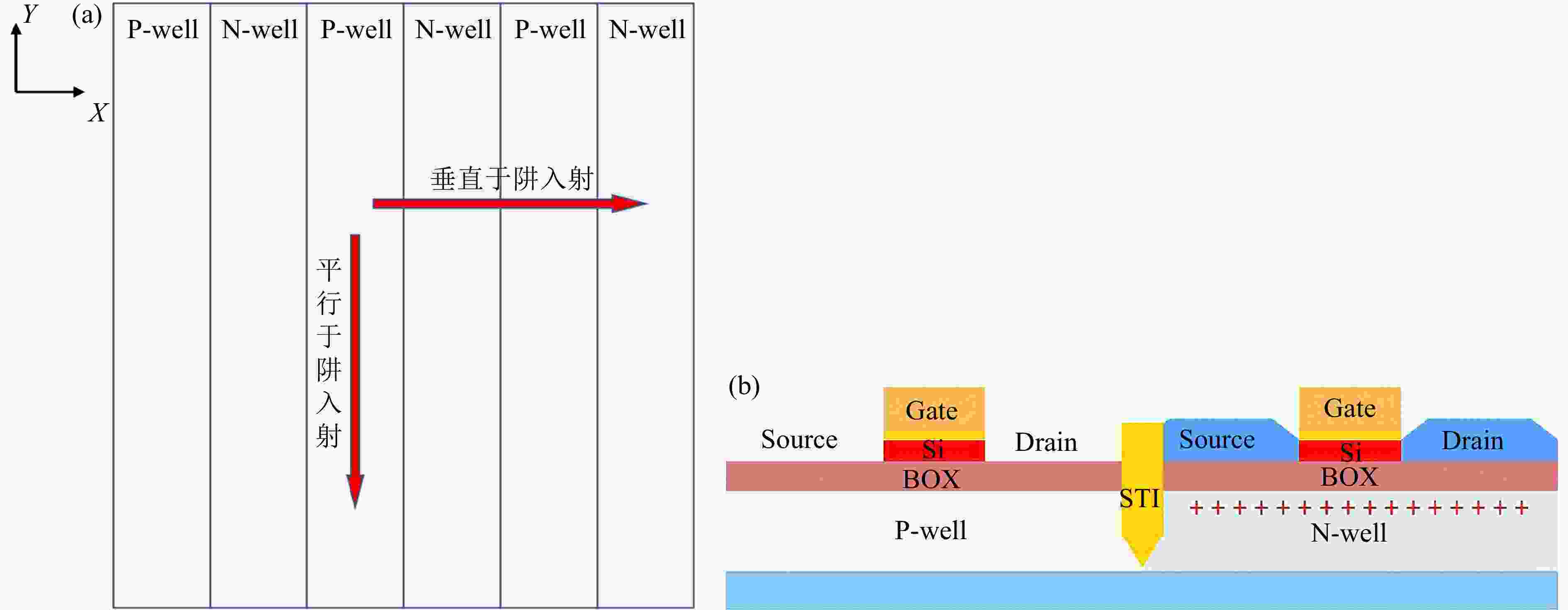
图 12 重离子入射方向与阱的相对位置(a)及FDSOI CMOS晶体管剖面图(b)(在线彩图)
图13为重离子平行于阱方向(α = 90°)和垂直于阱方向(α = 0°)入射的MCU比例。实验结果表明,当重离子垂直于阱方向入射,倾角β = 30°时,MCU比例出现了明显的增大现象。继续增大β到60°时,MCU比例与β = 30°时的比例基本一致。因此对于垂直于阱方向入射,MCU比例出现明显增大的β角度阈值在0°到30°之间。当重离子平行于阱方向入射,倾角β = 30°的MCU比例无明显变化,而β到60°的MCU比例出现了明显的增大。因此对于平行于阱方向入射,MCU比例出现明显增大的β角度阈值在30°到60°之间。总之,在考虑角度入射对器件可靠性影响时需要对更敏感的入射方向进行实验评估,并采取相应的版图加固措施。
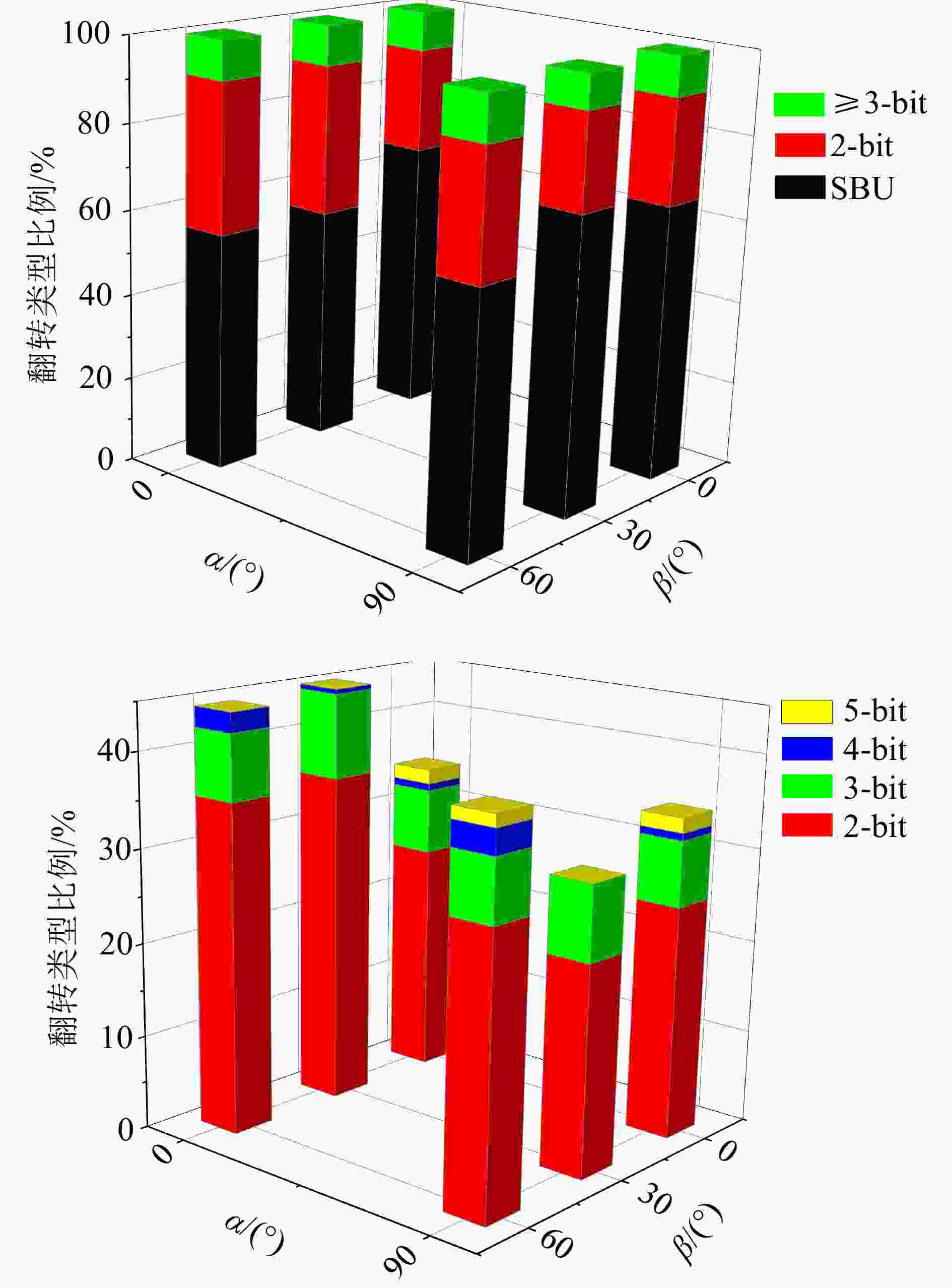
图 13 MCU比例随重离子入射角度的变化趋势(在线彩图)
根据角度依赖性的实验结果可以得出,重离子平行于阱方向[Y方向(α = 90°)]入射为“最劣入射方向”,沿此方向入射的倾角越大,SEU截面和MCU比例就越大,实验中平行于阱方向60°入射为此次结果的“最劣入射”。相比于“垂直入射”,“最劣入射”的SEU比特截面提高了152%,SEU事件截面提高了195%,MCU比例由原来的34%提升到了44%。因此,对于器件SEU可靠性评估,为了更加真实地模拟出空间重离子各向同性的特点,重离子斜角入射应该被更多地应用到器件的地面单粒子效应评估测试中。
-
本文开展了对22 nm FDSOI SRAM器件的LET、电压、角度等参数的SEU实验研究。实验结果表明,重离子LET增加会显著增大22 nm FDSOI SRAM的非直接扩散型电荷共享范围,进而使22 nm FDSOI SRAM器件的MCU事件发生率上升,且实验观察到的最大MCU事件为5位多单元翻转。因此,当重离子的电离径迹尺寸远大于器件的单元尺寸时,电离产生的高能δ电子会穿透氧化物隔离介质进入相邻单元,进而使完全隔离的单元间发生电离电荷共享;此外,当重离子沿平行于衬底阱区方向入射时,电离电荷沿阱区方向分布,且电离电荷扩散路径无STI阻挡。因此,重离子沿平行于阱区方向入射能够在22 nm FDSOI的BOX层下堆积更多的过程空穴,产生更大的扰动电场,进而拉低源体结和漏体结的势垒高度,增强了双极寄生电流。空间银河宇宙射线具有各向同性入射的特点,因此地面加速器实验测试FDSOI器件空间单粒子效应可靠性,必须评估高LET值区段的MCU位图及占比、以及离子入射方位角α和倾角β对直接沉积电荷和间接寄生电荷收集机制的影响。
-
摘要: 全耗尽绝缘体上硅(FDSOI)工艺是制备高可靠宇航电子器件的理想半导体工艺,因此深入揭示FDSOI工艺器件的单粒子效应机理对抗辐射加固设计具有理论指导意义。针对22 nm FDSOI SRAM测试器件,研究了不同重离子及电学参数对器件单粒子翻转敏感性的影响规律及物理机制。实验结果表明,高LET值区域单粒子多单元翻转事件占比可达20%,且核心电压对单粒子翻转类型比例及发生概率影响较小;重离子倾角入射会显著增大器件的单粒子翻转截面,且重离子沿平行与垂直衬底阱区方向入射时的单粒子翻转截面差异可达130%。因此,FDSOI器件单粒子效应建模及抗辐射加固设计,必须考虑非直接扩散型电荷共享机制、衬底电势畸变触发寄生电流机制对单粒子瞬态电离电荷收集过程的影响。Abstract: The Fully Depleted Silicon on Insulator(FDSOI) process is considered an ideal semiconductor technology for producing highly reliable aerospace electronic devices. Therefore, a comprehensive understanding of the single event effects mechanism in FDSOI devices is of theoretical significance for radiation-hardened design. This paper focuses on 22 nm FDSOI SRAM test devices and investigates the impact patterns and physical mechanisms of different heavy ions and electrical parameters on the sensitivity of Single Event Upset(SEU) in the devices. Experimental results indicate that in regions with high Linear Energy Transfer(LET) values, the proportion of Multi-Cell Upset(MCU) can reach 20%. Additionally, the core voltage has a relatively minor impact on the type proportion and occurrence probability of SEU. The incidence angle of heavy ions significantly increases the SEU cross-section of the devices, with a 130% difference observed when heavy ions are incident along parallel and perpendicular directions to the substrate well region. Therefore, when modeling Single Event Effect in FDSOI devices and designing for radiation hardening, it is imperative to consider the influence of non-direct diffusion charge sharing mechanisms and substrate potential distortion-triggered parasitic current mechanisms on the transient ionization charge collection process.
-
Key words:
- single event effect /
- heavy ions /
- multi-cell Upset /
- FDSOI /
- SRAM /
- angular incidence
-
表 1 SRAM实验条件及参数
实验条件 实验参数 角度/(°) α = 0,90;β = 0,30,60 核心电压/V 0.54,0.72,0.80,0.90,1.08,1.26 LET/(MeV·cm2·mg−1) 8.7,13.4,22.2,37.4,75.4,78.1  下载: 导出CSV
表 2 重离子辐照实验参数
离子
种类空气
厚度/mm铝箔
厚度/μm能量/MeV LET/
(MeV·cm2·mg-1)Si中
射程/μmTa 40 0 2 006.4 75.4 116.6 70 0 1 721.4 78.1 100.7 Al 0 0 110.0 8.7 48.0 Cl 0 0 150.0 13.4 42.8 Ti 0 0 160.0 22.2 32.9 Ge 0 0 205.0 37.4 30.0
下载: 导出CSV
-
[1] BARILLOT C, CALVEL P. IEEE Transactions on Nuclear Science, 1996, 43(2): 453. doi: 10.1109/23.490914 [2] BINDER D, SMITH E C, HOLMAN A B. IEEE Transactions on Nuclear Science, 1975, 22(6): 2675. doi: 10.1109/TNS.1975.4328188. [3] ECOFFET R. IEEE Transactions on Nuclear Science, 2013, 60(3): 1791. doi: 10.1109/TNS.2013.2262002. [4] HARBOE-SORENSEN R, POIVEY C, ZADEH A, et al. IEEE Transactions on Nuclear Science, 2012, 59(4): 1086. doi: 10.1109/TNS.2012.2185062 [5] SIMOEN E, GAILLARDIN M, PAILLET P, et al. IEEE Trans Nucl Sci, 2013, 60(3 Part2): 1970. doi: 10.1109/TNS.2013.2255313 [6] VITALE S, WYATT P, CHECKA N, et al. Proceedings of the IEEE, 2010, 98(2): 333. doi: 10.1109/JPROC.2009.2034476 [7] GASIOT G, SOUSSAN D, GLORIEUX M, et al. SER/SELPerformances of SRAMs in UTBB FDSOI28 and Comparisons with PDSOI and BULK Counterparts[C]//IEEE International Reliability Physics Symposium, New York: IEEE, 2014. [8] ASPRILLA A, CORDOVA D, DEVAL Y, et al. IEEE Transactions on Circuits and Systems II Express Briefs, 2021, 68(2): 602. doi: 10.1109/TCSII.2020.3047464 [9] SCHWANK J R, FERLET-CAVROIS V, SHANEYFELT M R, et al. IEEE Transactions on Nuclear Science, 2003, 50(3): 522. doi: 10.1109/TNS.2003.812930 [10] DAVIS G E, HITE L R, BLAKE T, et al. IEEE Transactions on Nuclear Science, 1985, 32(6): 4431. doi: 10.1109/TNS.1985.4334137 [11] MUSSEAU O. IEEE Transactions on Nuclear Science, 1996, 43(2): 603. doi: 10.1109/23.490904 [12] GASIOT G, SOUSSAN D, GLORIEUX M, et al. SER/SEL Performances of SRAMs in UTBB FDSOI 28nm and Comparisons with PDSOI and BULK Counterparts[C]//IEEE International Reliability Physics Symposium. New York: Institute of Electrical and Electronics Engineer Inc, 2014 [13] CAI Chang, ZHAO Peixiong, XU Liwei, et al. Microelectronics Reliablity, 2019, 100-101: 113322. doi: 10.1016/j.microrel.2019.06.014 [14] MALHERBE V, GASIOT G, SOUSSAN D, et al. Alpha Soft Error Rate of FDSOI 28 nm SRAMs: Experimental Testing and Simulation Analysis[C]. New York: IEEE, 2015. [15] HEIDEL DAVID F, MARSHALL PAUL W, PELLISH JONATHAN A. et al. IEEE Transactions on Nuclear Science, 2009, 56(6): 3499. doi: 10.1109/TNS.2009.2033796 [16] AKKERMAN A, BARAK J. Nuclear Science IEEE Transactions on, 2002, 49(6): 3022. doi: 10.1109/TNS.2002.805366 [17] GASPARD N J, JAGANNATHAN S, DIGGINS Z J, et al. IEEE Transactions on Nuclear Science, 2013, 60(6 Part1): 4368. doi: 10.1109/TNS.2013.2289745 [18] DENNARD R H, GAENSSLEN F H, YU H N, et al. IEEE Solid-State Circuits Society Newsletter, 2007, 12(1): 38. doi: 10.1109/N-SSC.2007.4785543 [19] RAINE M, HUBERT G, GAILLARDIN M, et al. IEEE Transactions on Nuclear Science, 2011, 58(6): 2607. doi: 10.1109/TNS.2011.2168238 [20] RAINE M, GAILLARDIN M, LAGUTERE T, et al. IEEE Transactions on Nuclear Science, 2017, 65(1): 339. doi: 10.1109/TNS.2017.2779786 [21] 赵凯, 高见头, 杨波, 等. 信息与电子工程, 2010, 8(01): 91. doi: cnki:sun:xxyd.0.2010-01-023 ZHAO Kai, GAO Jiantou, YANG Bo, et al. Information and Electronic Engineering, 2010, 8(01): 91. (in Chinese) doi: cnki:sun:xxyd.0.2010-01-023 [22] RAINE M, HUBERT G, GAILLARDIN M, et al. IEEE Transactions on Nuclear Science, 2011, 58(3): 840. doi: 10.1109/TNS.2011.2109966 [23] RAINE M, VALENTIN A, GAILLARDIN M, et al. IEEE Transactions on Nuclear Science, 2012, 59(6): 2697. doi: 10.1109/TNS.2012.2220783 [24] 贺泽. 纳米存储器件和组合逻辑器件的单粒子效应研究[D]. 兰州: 中国科学院近代物理研究所, 2022. HE Ze. Study of Single Event Effects on Nanoscale Memory Device and Combinational Logic Device[D]. Lanzhou: Institute of Modern Physics, Chinese Academy of Science, 2022. (in Chinese) [25] 莫莉华. 新型FinFET器件和3D堆叠器件的单粒子效应研究[D]. 兰州: 中国科学院近代物理研究所, 2021. MO Lihua. Investigation of Single Event Effects in New FinFET Device and 3D Stacked Device[D]. Lanzhou: Institute of Modern Physics, Chinese Academy of Science, 2021.(in Chinese) [26] 蔡畅. 纳米SRAM型FPGA的单粒子效应及其加固技术研究[D]. 兰州: 中国科学院近代物理研究所, 2021. CAI Chang. Study of Single Event Effects and Hardening Strategies on Nanoscale SRAM-based FPGA[D]. Lanzhou: Institute of Modern Physics, Chinese Academy of Science, 2021.(in Chinese) [27] ROCHE P, GASIOT G, FORBES K, et al. IEEE Transactions on Nuclear Science, 2003, 50(6): 2046. doi: 10.1109/TNS.2003.821588 [28] MERELLE T, SAIGNE F, SAGNES B, et al. IEEE Transactions on Nuclear Science, 2005, 52(5): 1538. doi: 10.1109/tns.2005.855823 [29] TIPTON A D, PELLISH J A, HUTSON J M, et al. IEEE Transactions on Nuclear Science, 2008, 55(6): 2880. doi: 10.1109/TNS.2008.2006503 [30] GIOT D, ROCHE P, GASIOT G, et al. IEEE Transactions on Nuclear Science, 2007, 54(4): 904. doi: 10.1109/tns.2007.902360 -

 点击查看大图
图(13) / 表 (2)
计量
- 文章访问数: 249
- HTML全文浏览量: 106
- PDF下载量: 16
- 被引次数: 0


 甘公网安备 62010202000723号